Cyber Resilience Act: New requirements for CE marking
From December 2027, IoT-enabled devices and networked industrial electronics may only be placed on the market with CE marking if their manufacturers provide evidence of effective protective measures against cyber attacks. "As the harmonized standards required for this are still being developed, many companies are faced with unanswered questions. Despite open standards, we already have to integrate cyber security into ongoing development projects because these products will then be launched on the market," says FED Advisory Board member Hanno Platz, describing the situation.
 FED Advisory Board member Hanno Platz: "The topic of cyber security must already be actively integrated into development processes nowTheEU Regulation 2024/2847 (Cyber Resilience Act, CRA) will require all manufacturers of electronic products with digital elements to implement comprehensive security measures from December 11, 2027. Products that fall under the scope of the CRA will then have to bear the CE marking in order to be placed on the market in the EU. In concrete terms, this means
- The CRA will become part of the EU approach to product safety, similar to the Low Voltage Directive or the Machinery Regulation.
- Manufacturers must prove that their product meets the requirements of the CRA in order to receive the CE marking.
- Without CE marking, products with digital elements may no longer be sold or put into operation from December 11, 2027 if they fall under the CRA.
- While CE primarily covered physical safety and electromagnetic compatibility in the past, the CRA introduces a new aspect:
- Cybersecurity becomes a mandatory requirement.
- Manufacturers must analyze risks, implement safety measures and document them.
- Requirements apply across the entire product life cycle: from development and updates to the reporting of security incidents.
All electronic interfaces and communication connections that a product with digital elements has are potentially subject to the CRA requirements, especially if they represent a gateway for cyber attacks. This is relevant for all IoT-enabled devices, networked industrial electronics, software in embedded systems and devices with wireless or wired communication interfaces. Manufacturers must systematically analyze these and take measures to ensure resilience.
FED Advisory Board members and regional group leaders Hanno Platz and Kostas Mouselimis have compiled a list of the typical interfaces and connections to electronics that fall under the CRA requirements. This overview on the FED website provides guidance as to which devices should be considered in particular.
Plant closure in Enns: Panasonic base material officially discontinued
FED board member and working group leader Sven Nehrdich 16 experts and FED members from the PCB industry discuss current and new projects, specifically theCO2 calculation for PCB manufacturers and consideration of the processing and cycle stability of stacked vias.
The supply situation with base material was also a topic. In February, Panasonic announced that it would be closing its plant in Enns, Austria, by the end of 2025. This plant produces base material for printed circuit boards - especially for the European market. The closure means that one of the last production sites for base material in Europe will no longer exist. At the same time, the material produced there has been officially discontinued.
Many PCB manufacturers with production facilities in Germany process the base material from Enns - the scope of this discontinuation is correspondingly large. The material is used in particular in applications with high reliability requirements, such as automotive or medical electronics.
Panasonic will supply the base material from Japan in future. However, despite its similar name, the material from Japan does not have the same properties as the product from the European production facility in Enns.
Switching to a different base material is technically and organizationally demanding. The materials consist of several components and have to undergo complex chemical and physical processes during production. To ensure the required electrical properties, an internal approval process is necessary at the PCB manufacturer. In addition, a new UL approval is often required - especially for PCBs that are exported to the North American market. External approval by the end customer is also necessary.
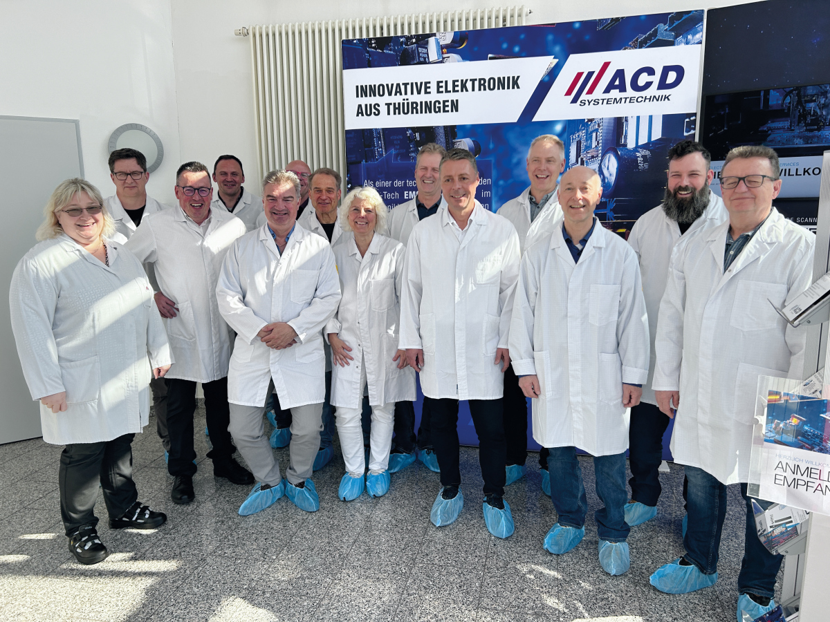 The spring meeting of the FED PCB working group took place in Neustadt/Orla
PEDC 2026 in Prague: Europe's design conference enters its second round
After a successful start with experts and industry representatives from 20 countries, the Pan-European Electronics Design Conference (PEDC) of FED and IPC will take place again on January 21 and 22, 2026 - this time in the heart of Europe: in Prague.
The PEDC brings together developers from all over Europe to discuss practical design concepts and efficient development processes from the chip to the end device and the challenges in hardware design as well as future-oriented solutions for industrial electronics. Join us as a participant or speaker. We are accepting proposals for English-language presentations for a 30-minute session until July 31. Or present your company as a sponsor or exhibitor.
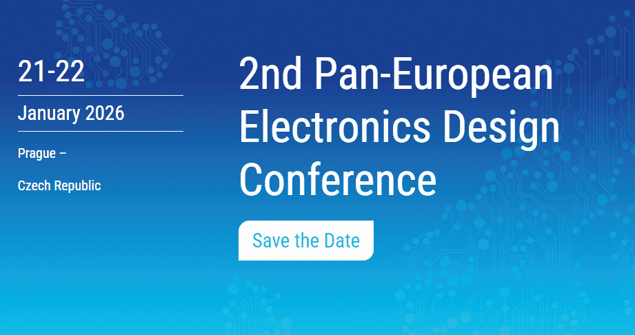 FED and IPC organize the new conference format
FED Conference 2025 in Lübeck: Where strong connections create new perspectives
 In his entertaining speech, Dr. Henning Beck shows what we have ahead of AI - and how we can use itWhatdistinguishes humans from machines - and how can we use this knowledge for real innovations in electronics? The 33rd FED Conference on September 24 and 25, 2025 in Lübeck is dedicated to precisely these questions under the motto "Strong Connections" - at a time when technological change, economic uncertainty and geopolitical unpredictability are challenging our industry like never before.
A highlight on the second day of the conference: Dr. Henning Beck, neuroscientist, biochemist and science slam champion, will open the day with a rousing keynote speech. He will show how the human brain makes mistakes in order to create something new - and why this is the decisive advantage over artificial intelligence. An impulse that stimulates and entertains. The rest of the program and the conference app include
- a large exhibition with over 40 stands
- 48 specialist presentations on PCB design, assembly production and technical management
- Networking in a Hanseatic maritime atmosphere at the evening event
- and, for the first time, presentations in English - for a stronger exchange at European level
- A focus on 3D electronics with five contributions curated by the FED working group on tools, materials and additive manufacturing processes
For the 33rd time, the FED Conference will bring together experts along the entire electronics chain and promote what really drives our industry: trust, dialog and joint solutions.
Impulses and dates by e-mail: The FED newsletter
Twice a month, the FED office provides experts in electronics design and assembly production with information, meetings of the FED regional groups and valuable impulses directly for downloading, registering or informing. The FED newsletter is free of charge and can be canceled at any time. To subscribe, simply enter your name and e-mail address at this link: www.fed.de/newsletter.
Calendar of events September and October 2025
| 1.-5.9 | ZED Level II - Printed circuit board assembly design 1, Neustadt/A. | 15.-17.9. | High-speed assembly design (ZED IV), Neustadt/A. |
| 8.-12.9. | ZED Level III - Printed circuit board assembly design 2, Neustadt/A. | 18./19.9. | EMC-compliant assembly design (ZED IV), Neustadt/A. |
| 9.9. | Signal Integrity Simulation in Practice, Berlin | 24./25.9. | 33rd FED Conference, Lübeck |
| 10.9 | Power Integrity Simulation in Practice, Berlin | 29.9.-1.10. | Cable Assembly Practice, Erlangen |
| 15.-18.9. | IPC-A-610 course for specialists, Fulda |
FED e. V., Frankfurter Allee 73c 10247 Berlin
Phone +49(0)30 3406030-50
Fax. +49(0)30 3406030-61
http://www.fed.de
email:


