CICMT 2022 - Ceramic Interconnect and Ceramic Microsystems Technologies
Vienna July 13 - 15, 2022
The international conference "Ceramic Interconnect and Ceramic Microsystems Technologies" (CICMT) will take place in Vienna in July. For many years, IMAPS USA, Asia and Europe have shared the venues. After 2 years of online events, the ceramic-electronic community is looking forward to a face-to-face event to exchange technical information and to network face-to-face again. We are looking forward to an exciting program, good keynotes, informative discussions and an interesting exhibition.

Christophe Moser, Associate Professor of Optics and Section Head at the Institute of Electrical Engineering and Microtechnology at EPFL, will give a presentation on "Volumetric 3D printing of high performance ceramics". During the lecture, he will present current methods of volumetric additive manufacturing (VAM). He will show examples of fabricated complex silicon oxycarbide ceramics with excellent performance in terms of heat and chemical resistance.
|
12:30 - 12:45 |
Welcome/ Opening Ceremony |
|
Ulrich Schmid, TU Vienna, Markus Eberstein, TDK Sensors AG & Co KG |
|
|
12:45- 13:45 |
Keynote 1: How to Improve Surface Functions Using Laser-based Fabrication Methods. New concepts and perspectives |
|
Andrés F. Lasagni, Technical University Dresden and Fraunhofer IWS |
|
|
14:15 - 16:45 |
Emerging Materials |
|
Session Chair:Jens Müller, TU Ilmenau, Ammar Kouki, Ecole de technologie supérieure |
|
|
Applications |
|
|
Session Chair:Soshu Kirihara, Osaka University, Uwe Partsch, Fraunhofer IKTS |
|
9:00 - 10:00 |
Keynote 2: Structured Glass Substrates for Packaging of Electronic Components |
|
Martin Letz, SCHOTT AG |
|
|
10:30 - 12:00 |
Integrated Passive Devices |
|
Session Chair:Camilla Kärnfelt, IMT Atlantique, Ulrich Schmid, TU Vienna |
|
|
Conductor Technology |
|
|
Session Chair:Markus Eberstein, TDK Sensors AG & Co KG, Ammar Kouki, Ecole de technologie supérieure |
|
|
13:30 - 15:00 |
Advanced Materials |
|
Session Chair:Dan Krüger, Honeywell, Jaroslaw Kita, University of Bayreuth |
|
|
Process Technology |
|
|
Session Chair:Ali Hajian, ams OSRAM, Steve Dai, Sandia National Labs |
|
|
15:30 - 17:30 |
Si-/LTCC-Compound Substrate Technology |
|
Session Chair:Achim Bittner, Hahn Schickard, Martin Letz, SCHOTT AG |
|
|
RF & Microwave |
|
|
Session Chair:Uwe Krieger, VIA electronic GmbH, Martin Oppermann, Hensoldt |
|
|
19:00 - 21:00 |
Conference Dinner |
|
9:00 - 10:00 |
Keynote 3: Volumetric 3D Printing of High Performance Ceramics |
|
Christophe Moser, EPFL |
|
|
10:30 - 1:00 |
Metallization Pastes |
|
Session Chair:Dawei Wang, Shenzhen Institute of Advanced Technology, Achim Bittner, Hahn Schickard |
|
|
Additive Manufacturing |
|
|
Session Chair:Ulrich Schmid, TU Vienna, Markus Eberstein, TDK Sensors AG & Co. KG |
|
|
13:00 - 13:15 |
Farewell/ Closing Ceremony |
|
Session Chair:Markus Eberstein, TDK Sensors AG & Co. KG, Session Chair:Ulrich Schmid, TU Vienna |
|
|
15:00 - 17:00 |
Visit of Lithoz |
Andrés F. Lasagni from Dresden University of Technology and Fraunhofer IWS will present new concepts and perspectives on "How to Improve Surface Functions Using Laser-Based Fabrication Methods" in his keynote lecture. Martin Letz from SCHOTT AG Mainz will give a lecture on "Structured Glass Substrates for Packaging Electronic Components". The semiconductor industry is gradually approaching the end of Moore's Law. This means that reducing the structure size on the silicon chip will no longer be the greatest lever for downsizing electronic components. Instead, heterogeneous packaging of active and passive components will become the focus in order to maximize performance, optimize yield and reduce the size of electronic components.
 Christophe Moser
 Andrés F. Lasagni
 Martin Letz
Following the IMAPS fall conference, we agreed to share selected topics here in our association section for all PLUS members and readers. In this context, the following two contributions were submitted, which we are pleased to present. Many thanks to the authors for publishing and adapting them to the journal format.
|
Venue: Austrian Federal Economic Chamber Vienna General Chair: Ulrich Schmid, TU Vienna Vice General Chair: Markus Eberstein, TDK Sensors You will find detailed information, the complete program and notes on the website https://imapseurope.org/event/cicmt-2022/ |
Ultrasonic wire bonding process: Efficient process development through simulation
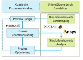 Fig. 1: Embedding the process model for ultrasonic thick-wire bonding in process developmentInnew generations of power modules with SiC semiconductors - e.g. as inverters for drives and converters in battery systems of electric vehicles - copper bonding wires are increasingly being used instead of the established aluminum bonding wires in order to improve reliability and service life. However, the higher mechanical strength of copper leads to higher process forces, which increases the risk of damage to the sensitive top side of the chip. These challenges must be overcome during process development, which is typically divided into three steps: process design, process characterization and process optimization. In process design, the new bonding process is designed in a target-oriented manner and, for example, the die top system, wire material and bonding tool are determined; for copper thick wire bonding, for example, die top systems with copper metallization and bonding tools with increased wear resistance are specifically selected. In 'Process Characterization', the bond quality is determined experimentally as a function of the process parameters (US power, bond duration, standard bond force, ...). In 'Process optimization', the analysis is then carried out using, for example, interaction and main effect diagrams in order to derive optimum process parameters with regard to the targets defined in the process design. If the targets are not achieved, iterations of the development process are necessary.
The successful and efficient development of new wire bonding processes according to the classical development scheme requires qualified know-how of the process developers, who select the design parameters in the first step and define test plans for the experimental characterization. Experimental 'process characterization' is a significant time and cost factor. The bond quality is determined by shear tests, microscope images, micrographs and complex lifetime tests such as active power cycling, whereby the tests are carried out manually and only partially automated.
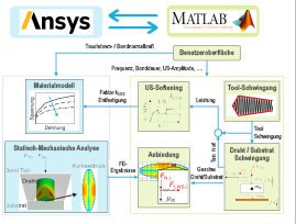 Fig. 2: Structure of the co-simulation of the process model: Thanks to the modular design, the model can be adapted and parameterized for different processes with limited effortIn order tokeep the scope of testing as small as possible and to be able to develop new bonding processes in a shorter time, a process model for ultrasonic thick-wire bonding was developed at the Chair of Dynamics and Mechatronics at Paderborn University. The embedding of the model in the development process is shown in Figure 1. The model is based on a co-simulation between the two programs MATLAB and ANSYS, see Figure 2. In MATLAB, computationally efficient models are used to calculate the transient dynamics of the process with the oscillations of the bonding tool, wire and substrate as well as the bonding process in the joining zone between wire and substrate for each oscillation cycle over the entire bonding time. In ANSYS, the finite element (FE) method is used to simulate the complex 3D wire deformation, which is influenced by the so-called ultrasonic softening effect in addition to the bond normal force. The FE calculation results in the contact surface and pressure distribution between the wire and substrate, which are incorporated into the bonding model. The process model outputs shear forces, shear strengths and other variables such as tangential force and vibration curves. The calculation is carried out in parallel on the university's own cluster computer resources(https://pc2.uni-paderborn.de), so that extensive parameter studies can be carried out in a significantly shorter time than experimental studies of the same scope. The simulation model makes it possible to evaluate a preselection of different bondtool designs or substrate clamping systems based on a model in the first process development step and to define parameter spaces for subsequent bonding tests. During the process characterization, the process model provides valuable additional information about the bonding process in the form of simulation results (force reactions, vibration curves, ...), which could only be determined experimentally to a limited extent and with very high experimental effort.
As an example of what the model provides, Figure 3 shows a comparison of the main effect diagrams from simulation and measurement. In the case of aluminum wire, the shear force in the area under consideration increases with increasing normal bond force, bond duration and ultrasonic voltage. The main influencing variable is the normal force. For copper wire, on the other hand, the normal bonding force has no significant effect on the shear force values. Bond duration and ultrasonic voltage cause an increase in the shear force; the ultrasonic voltage has the greatest influence here.
 Fig. 3: Simulatively and experimentally determined main effect diagrams for the single-phase ultrasonic bonding of 400 µm wire on DCB substrate: The significance of the parameters depends on the material and can already be evaluated in early process development phases based on models
The good agreement between simulated and experimentally determined main effect diagrams shows the potential of the process model, which can already be used in the early development phase to determine significant influencing variables on the bond quality.
Further information on the application of simulation models in ultrasonic wire bonding and welding can be found at: https://mb.uni-paderborn.de/ldm/forschung/sensorik-aktorik-und-ultraschalltechnik.
Julian Schirmer
Marcus Reichenberger
Production of mechatronic modules using printing technologies, high-pressure forming and back injection molding
Nuremberg Institute of Technology Georg Simon Ohm can look back on the successful completion of the "MecDruForm" research project (joint project "IngenieurNachwuchs2016" in the "Research at Universities of Applied Sciences" program, funded by the Federal Ministry of Education and Research under the funding code 03FH020IA6), which was carried out from 2017 until the end of 2021 in the laboratory for assembly and joining technology at the TH in cooperation with one research and two industrial partners. The use of printed electronics in combination with high-pressure forming and back injection molding enabled the successful production of three-dimensional mechatronic assemblies. The first sample assemblies demonstrate the suitability of the process chain developed in the project.
Starting point and motivation
The growing demand for miniaturized and highly integrated mechatronic modules means that in addition to the electrical function, mechanical, thermal or optical functions must increasingly be fulfilled by the circuit carrier. For some years now, spatial, injection-molded circuit carriers (MIDs) have increasingly been used for this purpose. However, when manufacturing such MIDs using established industrial processes, very specific processing conditions must be met. The BMBF research project "MecDruForm" therefore investigated in detail how these restrictions can be avoided by using synergistically coordinated alternative production methods. The research hypothesis on which the project is based can be illustrated by the process chain shown in Figure 4: Three-dimensional mechatronic assemblies can be produced from circuit carriers structured using printing technology and subsequently assembled by means of high-pressure forming and back injection molding.
 Fig. 4: Process chain for the production of thermoformed 3D mechatronic assemblies in the MecDruForm project
Initially, printed circuit carriers are built up on polymer substrates in the plane, whereby the advantages of standard system technology (screen and stencil printing, component placement and oven processes) can be utilized. The shape of the assembly is only created after the electrical properties have been produced by means of high-pressure forming. In the final step, these previously formed assemblies are encapsulated on the component side by means of injection molding and fixed in their shape, resulting in a fully functional three-dimensional assembly with a closed surface.
Project approach and selected results
![Abb. 5: SMD-Bauteilmontage auf gedruckter Elektronik; Substrat PET: leitgeklebte CR0603 (a), mit SnBiAg-gelötete CR0603 (b) und Schliffbild eines gelöteten DFN; pitch 0,5 mm (c) [1, 2]](/images/stories/Abo-2022-06/plus-2022-06-0028.jpg "Abb. 5: SMD-Bauteilmontage auf gedruckter Elektronik; Substrat PET: leitgeklebte CR0603 (a), mit SnBiAg-gelötete CR0603 (b) und Schliffbild eines gelöteten DFN; pitch 0,5 mm (c) [1, 2]") Fig. 5: SMD component assembly on printed electronics; PET substrate: conductively bonded CR0603 (a), CR0603 soldered with SnBiAg (b) and micrograph of a soldered DFN; pitch 0.5 mm (c) [1, 2]Using screen printing technology, the circuit layout is transferred to the flexible, dielectric film substrate using polymeric, Ag-filled thick-film pastes and the circuit carrier is metallized in a structured manner. Printed capacitive sensors are also realized. Once the printed layer has hardened, electronic components are mounted on the flat, flexible circuit carrier using SMD technology. The components used in the project range from passive components of size CR0805 and CR0402 to ICs in QFN packages with pitches of up to 0.5 mm. The components are contacted either by conductive adhesive technology at curing temperatures of around 150°C or by reflow soldering using low-melting SnBiAg solders at peak temperatures of around 170°C. However, the prerequisite for this solution is the wettability of the polymer thick-film pastes used and the thermal resistance of the film substrates in the reflow process. Figure 5 shows examples of suitable material combinations for AVT on printed electronics, as used in the project [1, 2].
Fig. 5: SMD component assembly on printed electronics; PET substrate: conductively bonded CR0603 (a), CR0603 soldered with SnBiAg (b) and micrograph of a soldered DFN; pitch 0.5 mm (c) [1, 2]Using screen printing technology, the circuit layout is transferred to the flexible, dielectric film substrate using polymeric, Ag-filled thick-film pastes and the circuit carrier is metallized in a structured manner. Printed capacitive sensors are also realized. Once the printed layer has hardened, electronic components are mounted on the flat, flexible circuit carrier using SMD technology. The components used in the project range from passive components of size CR0805 and CR0402 to ICs in QFN packages with pitches of up to 0.5 mm. The components are contacted either by conductive adhesive technology at curing temperatures of around 150°C or by reflow soldering using low-melting SnBiAg solders at peak temperatures of around 170°C. However, the prerequisite for this solution is the wettability of the polymer thick-film pastes used and the thermal resistance of the film substrates in the reflow process. Figure 5 shows examples of suitable material combinations for AVT on printed electronics, as used in the project [1, 2].
The SMT process chain is completed by the localized application of a potting compound in the area of sensitive components, which serves to protect them during further processing.
Three-dimensional shaping is then carried out on the fully assembled and already functional assemblies using high-pressure forming. Here, the assembly is first heated above the glass transition temperature (140°C to 160°C) of the amorphous film substrates and then formed under high pressure (30 bar to around 50 bar). A particular challenge here is that the entire circuit layout is deformed, which poses a local risk of damage to the conductor pattern and the connection points. Forming simulations, which were carried out in the project by the research partner Hof University of Applied Sciences, are therefore already necessary in the planning phase of product development in order to optimally adapt the circuit layout to the subsequent thermoforming loads. Detailed investigations were also carried out in the project in order to determine, for example, the change in resistance of printed conductor structures depending on the local degree of forming. Specific layout and process recommendations were derived from the results. For example, the use of meandering conductor structures reduces or prevents damage caused by cracking in areas subject to high stress during forming. Component connections also have an increased tendency to fail, which is why potting compounds were applied for local component protection, as mentioned above. With the material combinations used in the project, electronic components can be attached up to around 10%, and special meandering conductor runs up to 15% local deformation without loss of function [3, 4].
In the final step, these formed assemblies are reinforced by back-molding with thermoplastic material, creating an integrated three-dimensional mechatronic assembly. By selecting suitable overmoulding materials, other functions, such as thermal and optical ones, can be realized in addition to mechanical ones. Similar to the previous forming process, the overmolding process causes thermal and mechanical stresses for components and the conductor pattern. The molten plastic is injected at temperatures of around 300°C into a mold tempered at 80°C, which induces thermomechanical stress on the circuit pattern or the AVT, depending on the speed of the molten polymer. Due to the rapid cooling and the associated change in viscosity of the melt, the positioning and fixing of the formed circuit carrier in the mold is also an important factor. These points must also be taken into account in the planning phase, for example through simulations.
Discussion and summary
The research hypothesis formulated at the beginning of the project was confirmed. The technology demonstrator developed and shown in Figure 6 summarizes the results achieved. Various electronic components were installed in this 3D gaming device "TicTacToe", with printed capacitive sensors acting as operating and control elements. The assembly is characterized by the media-tight integration of the electronics, a closed surface and the integration of optical and mechanical functions. Important project results are highlighted as detailed images: Areas with high local forming could be overcome in a process-safe manner using meandering conductor tracks, the local use of protective materials reduced damage during the forming and overmoulding process and the contacting of highly miniaturized logic components with the smallest grid dimensions on screen-printed conductor structures was successfully implemented.
, dispenstes Verstärkungsmaterial im Bereich empfindlicher Bauteile vor dem Umspritzen (b) und Verwendung von Logikbauteilen mit kleinem Rastermaß (c)") Fig. 6: 3D gaming device "TicTacToe" as a demonstrator in the MecDruForm project; illustration of important project results through meandering conductor paths in areas with high local forming (a), dispersed reinforcement material in the area of sensitive components before overmolding (b) and use of logic components with small grid dimensions (c)
Fig. 6: 3D gaming device "TicTacToe" as a demonstrator in the MecDruForm project; illustration of important project results through meandering conductor paths in areas with high local forming (a), dispersed reinforcement material in the area of sensitive components before overmolding (b) and use of logic components with small grid dimensions (c)
By integrating electronic components, the approach successfully developed in the project goes far beyond what is currently understood by conformable electronics. Possible areas of application that could benefit from the new process chain include control elements for devices, lighting, assemblies in the automotive sector and medical products.
Partners
The research project was carried out by the research partners Institute of Materials Science (ifm) at Hof University of Applied Sciences, the Institute of Chemistry, Materials and Product Development (OHM-CMP) at Nuremberg Institute of Technology and two industrial project partners. From the industrial side, the companies Micro Systems Engineering GmbH (Berg) and RF Plast GmbH (Gunzenhausen) are supporting the research project.
References
[1] Schirmer, Julian; Eisen, Kilian; Reichenberger, Marcus; Roudenko, Jewgeni; Neermann, Simone; Franke, Jörg: Long-Term Behavior of SMT Components Mounted on Printed Polymer Thick Film Pastes, 13th International Congress Molded Interconnect Devices (MID), 2018
[2] Schirmer, Julian; Reichenberger, Marcus; Neermann, Simone, Franke, Jörg: Solder joints on polymer thick film pastes: Processing and properties, GMM-Fb. 94: EBL 2020 - Elektronische Baugruppen und Leiterplatten, VDE Verlag, 2020, pp. 43-48
[3] Schirmer, Julian; Reichenberger, Marcus; Neermann, Simone; Franke, Jörg: Conformable Electronics: Thermoforming and Injection Molding of Electronic Components, 44th International Spring Seminar on Electronics Technology (ISSE), 2021
[4] Schirmer, Julian; Reichenberger, Marcus; Wimmer, Annette; Reichel, Herbert; Neermann, Simone; Franke, Jörg: Evaluation of Mechanical Stress on Electronic Assemblies During Thermoforming and Injection Molding for Conformable Electronics, 14th International Congress Molded Interconnect Devices (MID), 2021

Calendar of events
|
Place |
Period |
Event name |
Organizer |
|
Vienna, AT |
July 13-15, 2022 |
CICMT 2022 |
IMAPS |
|
Sibiu, RO |
September 13-16, 2022 |
ESTC 2022 |
IEEE-CPMT IMAPS Europe |
|
Berlin, Germany |
Sept. 26-29, 2022 |
ESREF 2022 |
IZM / TU |
|
Boston, MA |
October 3-6, 2022 |
International Symposium |
IMAPS US |
|
Munich, Germany |
October 20/21, 2022 |
Fall Conference |
IMAPS D |
|
Munich, Germany |
November 15-18, 2022 |
SEMICON EUROPE |
SEMI Europe |
IMAPS Germany - Your association for packaging and interconnection technology
IMAPS Germany, part of the International Microelectronics and Packaging Society (IMAPS), has been the forum in Germany for all those involved in microelectronics and packaging technology since 1973. With almost 300 members, we essentially pursue three important goals:
- we connect science and practice
- we ensure the exchange of information among our members and
- we represent the position of our members in international committees.
Imprint
IMAPS Germany e. V.
Kleingrötzing 1, D-84494 Neumarkt-St. Veit
1st Chairman: Prof. Dr.-Ing. Martin Schneider-Ramelow, Deputy Director of the Fraunhofer Institute for Reliability and Microintegration (IZM),
Treasurer
(for questions about membership and contributions):
Ernst G. M. Eggelaar,
You can find detailed contact information for the board members at www.imaps.de
