Review of the 'NordPac 2022 Annual Microelectroninics and Packaging Conference and Exhibition' at Chalmers University of Technology in Gothenburg, Sweden
From June 12 to 14, 2022, almost 100 experts came together for the fourth 'NordPac 2022 Annual Microelectronic and Packaging Conference and Exhibition' at Chalmers University of Technology in Gothenburg, Sweden, after a two-year break due to the pandemic. The meeting was organized as a joint project by both the IEEE EPS Nordic and the iMAPS Nordic Chapter.
 Fig. 1: Founding certificate ISHM
The conference was accompanied by a trade exhibition with a total of 11 international exhibitors, who covered the entire spectrum of microsystems technology and presented it in an exhibitor session. Renowned companies such as ASE, MST, PacTech and AEMtec (Packaging), RoodMicrotec and eurofins-MASERE (Test & Reliability) as well as inseto and ROARTIS (Components & Consumables) were present.
Heidi Lundén (Schott Primoceler Oy), Chair of the iMAPS Nordics Chapter, opened the conference by welcoming the participants and emphasizing the ever-increasing need for improvement and further development in microsystems technology in order to meet the upcoming challenges in terms of reliability, cost efficiency and sustainability.
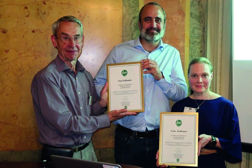 Fig. 2: Paul Colander, Daniel Nilsen Wright, Heidi Lundén
E. Jan Vardaman from TechSearch International took up this challenge in her keynote speech and, in an impressively comprehensive and detailed presentation, highlighted the future trends in packaging as well as assembly and connection technology to meet the requirements of 5G/6G communication, e-mobility, autonomous driving and IoT. In her opinion, technologies such as silicon interposers, fan-out on substrate, embedded bridges, RDL interposers and 3D stacking are becoming increasingly important. This keynote speech also laid the foundation for the technical session, which focused on the topics of error analysis & reliability and advanced packaging solutions in a total of 11 specialist presentations. A successful day 1!
Day 2 of the conference was then opened with the keynote speech by Andreas Ostmann from the Fraunhofer Gesellschaft IZM. The topic of the keynote: Pill Microsystems for Diagnostics and Therapy. A technology that was conceived at the end of the last century and proven to be functional in various prototypes and clinical studies at the beginning of this century, but despite its undoubtedly great advantages in terms of personalized diagnosis and medication, has not yet been able to make the breakthrough into the mass market. Decisive factors for this include size, functionality and cost. There is still great potential for development here for all participants involved in microsystems technology in order to ultimately lay the foundations for a 5_USD device. The subsequent technical presentations, which focused on thermal management and new materials, also addressed this topic.
The event was rounded off with a conference dinner in the historic Chalmerska Huset. In addition to the desired networking character, the participants were able to celebrate the 50th anniversary of the iMAPS Nordic Chapter a year late. Founded on May 5, 1971 as the International Society for Hybrid Microelectronics ISHM, iMAPS Nordics has existed since 1998 as a merger of the ISHM and the IEPS.
Paul Collander, long-standing chairman of the IMAPS Nordic Chapter, was bid farewell during the event. He was awarded honorary membership by Heidi Lundén and Daniel Nilsen Wright for his outstanding work.
Microgalvanic method for the deposition of laterally distributed layer thicknesses using an electroplating technology
T. Döhlera, A. Böhmea, J. Neumannb, R. Bochemb, M. Hofmanna, A.-H. Foitzika, U. Geisslera
aTechnical University of Applied Sciences Wildau, b Schiefer & Co (GmbH & Co.)
Abstract
This paper presents an electrochemical coating process for the deposition of visually unrecognizable, laterally distributed surface structures [1]. Concepts were created using real data from electrochemical simulations and transferred to a specially developed setup. With the parameters determined, it was possible to deposit an adhesive gold electrolyte on the cathode-side substrates (silver, nickel). The special arrangement and characteristics of the anode-side electrode geometries are important for the deposition process. These layers and their local distributions were investigated and verified using confocal laser microscopy, X-ray fluorescence analysis and laser interference measurements.
Introduction
In industrial applications, there are influencing variables and effects that must be prevented or at least reduced to ensure good product quality. One of these disturbance variables, the so-called 'dog bone' effect [2], leads to non-uniform layers as a result of the primary current distribution due to geometric changes and non-uniformities between the electrodes [3]. This is extremely undesirable in modern electrochemical coating technology. In electrochemical setups, attempts are therefore made to achieve parallelization of the field lines at the cathode by arranging the electrodes on the anode side or by inserting anode grids in order to prevent this effect.
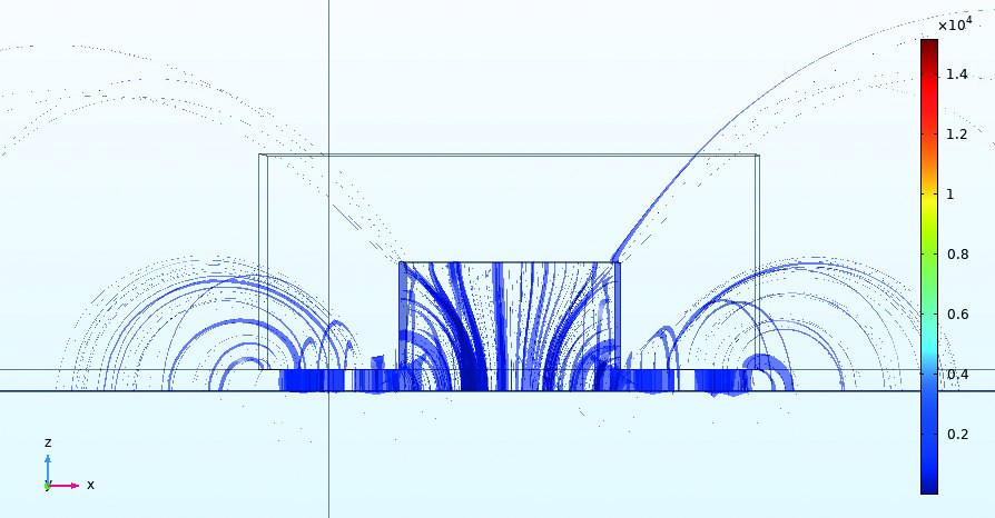 Fig. 1: Simulated distribution of the resulting field line density function in the process bath as a function of the anode geometry 'slot', distance d-700 µm, exaggerated representation of the increased deposition rate due to the field line density increase as a result of the anode geometry (simulation in Comsol Multiphysics, electrode position module)
This undesirable effect is used in reverse in the development presented in order to create an area in addition to the usual coating that is dependent on the influence of this geometric edge effect and allows a type of inhomogeneously distributed coating.
Materials and methods
The structures on the process-determining anode electrodes were produced using a microfabrication center (Kern Micro, Kern, Eschenlohe, Germany). The electrode materials were defined as platinum on the anode side and silver, gold and nickel on the cathode side. To reduce interfering influences, an electrolyte without additives (Wieland AC3 adhesive gold bath) was used. Structured rod electrodes were used on the anode side. The substrate electrode on the cathode side was made of silver and on the anode side of platinum. For the experimental investigations, the deposition area on the cathode side was limited to 1 cm² and the layer height to a maximum of 2 µm. An electroplating laboratory prototype was developed as a test setup, which made the process control and process parameterization adjustable. The close proximity of the electrodes to each other and the adjustment of the electrode spacing could be realized using micrometer units. The generated CAD models of the electrodes were transferred to the simulation software (Comsol Multiphysics, Electrodeposition module) and calculated as a model for adjusting the process parameters depending on the anode-side geometries and the cathode-side layer distribution(Fig. 1). The layers produced were analyzed using a laser confocal microscope (qualitative), X-ray fluorescence analysis (lateral layer thickness measurement) and interference measurement.
Results and discussion
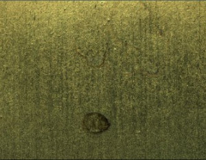
Figure 2 illustrates a substrate sample of an anode mold (groove). Roughness (Ra < 2 µm) and purity requirements were specified for the substrate materials so that the changed deposition character was more controlled and the distribution of the field lines was more homogeneous in addition to the forced field distribution. The samples shown were prepared at room temperature ~20 °C, U = variable, I = 0.5 mA, t =30 min, d = 700 µm with stirrer. In the optical analysis and using a laser confocal microscope (VKX-1100), these showed no visible evidence of structural variation in the layer thickness formation (see Fig. 2a). The profile measurements over the relevant layer areas also showed no significant changes. Black edges' were recognizable, which can be explained as edge effects due to gas bubble formation on the coating surface during the process. Despite agitation during the process, these were adhered to due to high capillary forces between the electrodes and could not always be avoided even with agitation.
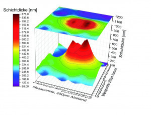
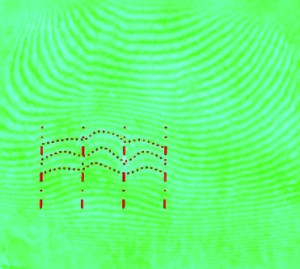
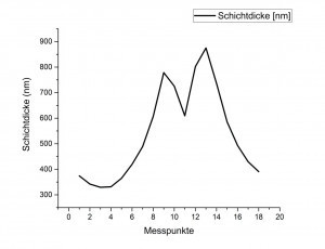
Fig. 2: Substrate sample rod electrode (groove): Optical inspection of the sample set using the LSM (a), analysis of the coating result of the groove anode geometry using XRF (c, d) in the 250 µm measuring range in the XY direction, display and evaluation of the XRF measurement results in the Originlab 3D software (c), line diagram (d), interferogram (b) of the anode geometry (groove)
In order to be able to analyze further conclusions about the layer behavior, the total layer thicknesses of the deposited layers were determined on selected sample sets using X-ray fluorescence analysis (XRF). The measuring points were placed in a matrix in such a way that they could map at least half of the relevant geometries of the respective production anode. The measuring range in the XY direction was 250 µm. The graphics shown in Figure 2c show the assumed and simulated coating thickness distribution in the 3D representation and the projected surface representation, or in the line diagram(Fig. 2d). The increase in layer thickness growth along certain geometry edges of the structured anode was caused by the compression of the field lines and the increase in streamline density. Figure 2c shows the geometry (groove) by forming two elevations.
An optical module for interference measurement was developed as part of the research project in order to provide as many users as possible in small and medium-sized companies with a cost-effective analysis option. This enables a qualitative analysis of the surface, in which the inhomogeneous gradual layer thickness distribution is immediately visualized. Figure 2b shows the interference image caused by the different layer thickness distribution on the coated surface. In the course of the project, the effect of processing could always be demonstrated in the first instance with the help of this self-developed optical interference detection method.
In general, the larger the structured area, the higher the current intensity must be in order to achieve the same current densities and the same or similar deposition results. With increasing distance, the expected homogenization of the field lines and a reduction of the gradual coating effect occurred.
Summary and outlook
It was possible to produce structures on metallic sample bodies by means of galvanic process technology using the reverse 'dog bone' effect. These are invisible to the naked eye, form a microstructured anode geometry and could be detected and described using conventional analysis methods and an interference detection module. The development enabled the necessary anodes to be produced using a combination of calculation, simulation and production technology. On the cathode side, a process for deposition on a planar surface was developed. In future work, the technology is to be transferred to other substrate materials and electrolyte types. The application of the novel process technology presented can support applications in the printed circuit board industry, photonics and optics, for example, or in practical applications in connection with digitization.
The authors would like to thank the German Federal Ministry for Economic Affairs and Energy (ZIM, AiF) for their financial support (Fkz.: ZF4012231DF8).
Logos of the funding bodies and project partners
Calendar of events
|
Location |
Period |
Event name |
Organizer |
|
Vienna, AT |
July 13-15, 2022 |
CICMT 2022 |
IMAPS |
|
Sibiu, RO |
September 13-16, 2022 |
ESTC 2022 |
IEEE-CPMT IMAPS Europe |
|
Berlin, Germany |
Sept. 26-29, 2022 |
ESREF 2022 |
IZM / TU |
|
Boston,MA |
October 3-6, 2022 |
International Symposium |
IMAPS US |
|
Munich, Germany |
October 20/21, 2022 |
Fall Conference |
IMAPS D |
|
Munich, Germany |
November 15-18, 2022 |
SEMICON EUROPE |
SEMI Europe |
This calendar is subject to change. Please note the information and notes of the organizers on the respective websites!
IMAPS Germany - Your association for packaging and interconnection technology
IMAPS Germany, part of the 'International Microelectronics and Packaging Society' (IMAPS), has been the forum in Germany for all those involved in microelectronics and packaging technology since 1973. With almost 300 members, we essentially pursue three important goals:
- we connect science and practice
- we ensure the exchange of information among our members and
- we represent the position of our members in international committees.
Imprint
IMAPS Germany e. V.
Kleingrötzing 1, D-84494 Neumarkt-St. Veit
1st Chairman: Prof. Dr.-Ing. Martin Schneider-Ramelow, Deputy Director of the Fraunhofer Institute for Reliability and Microintegration (IZM),
Treasurer
(for questions about membership and contributions):
Ernst G. M. Eggelaar,
You can find detailed contact information for the board members at www.imaps.de
(Board of Directors)

