IMAPS Fall Conference 2022
Munich, October 20-21, 2022
The IMAPS Germany Autumn Conference is an important platform for professional discussions between industry and academia as well as production and research in order to further strengthen and promote Germany as a business location. The conference offers the proven mix of professional exchange, personal interaction, exhibition, lecture series and consolidation of networks.
The focal points of the conference are:
- Design, modeling, simulation in assembly design
- Materials, processes, joining technologies
- System integration technologies
- Quality and reliability.
The conference is currently planned as a face-to-face event in Munich. If it cannot take place in person, the conference will be held on an online platform.
Please use the following link to register: https://www.conftool.net/imaps-herbstkonferenz-2022
CICMT 2022 review
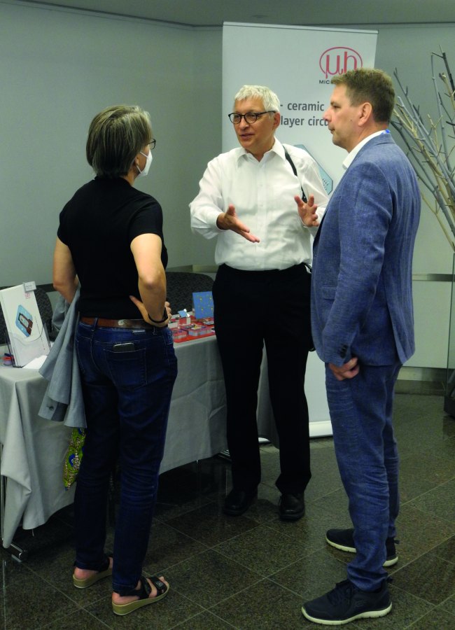
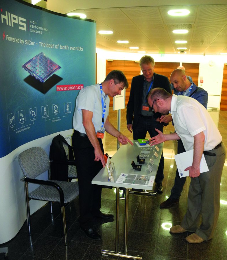
After two years of online events, the international CICMT conference ('Ceramic Interconnect and Ceramic Microsystems Technologies') was held in Vienna from July 13 to 15, 2022 in a face-to-face format again. It was organized by IMAPS Germany in cooperation with the Vienna University of Technology and held on the premises of the Austrian Federal Economic Chamber. The almost 80 participants from 12 countries were looking forward to the opportunity for face-to-face exchange and networking. Seven exhibitors - Lithoz, HIPS Wachstumskern, Micro-Hybrid Electronic, Keko Equipment, Microtronic, Budatec and F&S BONDTEC - supported the event and presented their products and services at the accompanying trade exhibition.
 The conference was accompanied by a trade exhibition at which seven companies and institutions presented their products
 Over the three days of the conference, a total of 40 lectures were presented in 10 parallel technical sessions covering a wide range of topics: New Materials, Applications, Integrated Passive Devices, Metallization, Process Technology, Si/LTCC Substrates, RF and Microwave Technology and Additive Manufacturing. The German community was the most strongly represented with 23 presentations, followed by Slovenia (4), USA (4) and Austria (3).
Each day the program was introduced with a keynote presentation. The first plenary lecture by Andrés-Fabián Lasagni from TU Dresden, one of the directors of the Center for Advanced Micro-Photonics, was dedicated to the topic 'How to Improve Surface Functions Using Laser-Based Fabrication Methods'. The Direct Laser Interference Patterning method in particular can contribute to the fast and effective surface treatment of different substrate materials. In this process, two to three laser beams are superimposed on the object surface. The resulting interference patterns have a striped or grid structure and can simultaneously generate up to 1 million individual dots per square millimeter. The aim is to functionalize the surface properties for the desired application; in particular, water wettability, biocompatibility and color can be modified using the process.
In the second keynote, 'Structured Glass Substrates for Packaging of Electronic Components', Martin Letz from SCHOTT AG reported on his company's new developments in the field of high-performance electronic substrates. Although glass has been used as a substrate material for electronic circuits for some time, it is only the latest technological advances that allow glass to be considered as a potential alternative for the production of rewiring layers with a high density of vias.
 The increasing demand for high-performance computing, driven primarily by applications such as autonomous driving and machine learning, is leading to the need for further miniaturization. This is not only about miniaturization in monolithic integration, but increasingly about the miniaturization of the package: the use of chiplets, ever higher switching and operating frequencies, lead to the need to reduce the connection length between the elements of the system in order to minimize power loss. The interposer solutions based on organic and ceramic PCBs have to give way to the silicon interposer in high-power areas, but the silicon-based solution is associated with high costs. As Mr. Letz has shown, glass can potentially replace silicon at only 10% of the cost.
The main problem with patterning glass is the loss of mechanical stability due to the introduction of surface defects in the process. The recently introduced SCHOTT FLEXINITY glass substrates remain defect-free even after the creation of cut-outs and drill holes; the glass wafer remains mechanically stable enough to be subjected to further process steps after laser processing. With the FLEXINITY Connect technology variant, more than 1 million vias with a diameter of up to 50 µm (via pitch from 1.5 times the diameter value) can be realized with a substrate size of over 500 mm and a thickness of 540 µm.
Since glasses with a wide range of electrical and mechanical properties are available, applications with a very broad spectrum can be realized: in addition to packaging for high-performance computing, for example, 5G and 6G modules with the corresponding antenna structures can be implemented, LiDAR and radar as well as medical applications are also possible. The main difficulties for widespread use are said to be the current lack of technological maturity in substrate metallization and still poorly developed production logistics.
 Technical papers were presented in two parallel sessions
 The conference dinner in the traditional 'Schweizerhaus' at the Vienna PraterThethird plenary lecture 'Volumetric 3D Printing of High Performance Ceramics' by Christophe Moser from the École polytechnique fédérale de Lausanne was dedicated to technologies for the additive manufacturing of ceramic products. The focus was on volumetric printing using tomographic back projection. In the volumetric curing of photopolymers, the three-dimensional shape of the object must be generated by the corresponding spatial intensity distribution in the volume of the photopolymer. This can be done, for example, by computer-generated holographic projection, but the available resolution of the projection systems is far from sufficient to enable a practically relevant application. For this reason, tomographic rear projection is currently used as an alternative method.
The principle can be most simply understood as the reversal of a tomographic image. In this approach, a cylindrical vessel filled with a liquid photopolymer is rotated around the vertical axis and exposed laterally with the projection of the object corresponding to the current angle. If the light dose is correctly adjusted to the photosensitivity of the emulsion, the three-dimensional object is produced as a hardened polymer after one or a few full rotations. Ceramic 3D bodies can also be produced with this process, using a so-called 'proceramic polymer', which can be converted into a ceramic structure after polymerization by decomposition. In his lecture, Mr. Moser presented several examples of printed three-dimensional objects made of silicon oxycarbide ceramics and quartz glass. The limitations of the volumetric method presented are currently mainly due to the limited number of materials that can be used - the photosensitive emulsion must have high transparency and be viscous. Although methods for compensating for the scattering in the liquid already exist, they are effective for the time being at the low concentration of the scattering particles.
The guided tours of the Vienna-based company Lithoz, which were organized in addition to the lecture sessions, were very well received by the conference participants. Lithoz GmbH is the global market and innovation leader in machines and materials for additive ceramic manufacturing using the LCM method (Lithographic Ceramic Manufacturing). Founded in 2011 as a spin-off of the Vienna University of Technology, the company has developed into an important player in the industry and was recognized as one of the five best Austrian start-ups in 2021 by the Spinn-Off Austria initiative.
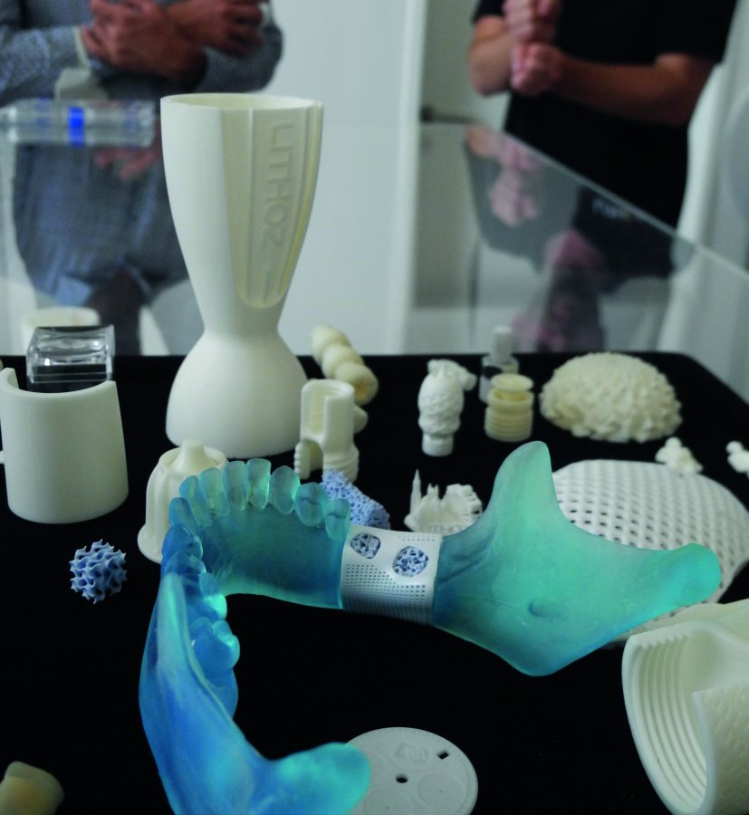
 Guided tour at Lithoz GmbH in ViennaThevisitors were able to see the machines of the CeraFab and CeraFab Multi series in action. The broad portfolio of available materials for many possible areas of application was presented on the basis of numerous samples. Lithoz, for example, supplies material solutions for 3D printing from standard ceramics such as aluminum oxide, zirconium dioxide and silicon nitride. The typical relative densities of more than 99% are achieved, while the mechanical and electrical properties correspond to those of conventionally produced ceramics. In the medical sector, tricalcium phosphate and hydroxyapatite are used as bone substitutes and in patient-specific resorbable implants.
IMAPS Germany will be holding one more conference this year - the traditional fall conference in Munich on October 20 and 21. The next Ceramic Interconnect and Ceramic Microsystems Technologies Conference will be held on May 8-11, 2023 in Albuquerque, USA together with HiTEC and Power Packaging. Make a note of the dates!
Glass now electrically conductive - new process enables integrated metallic microstructuring in glass for sensor technology
Protected from environmental influences, electrically and thermally conductive and lithographically very finely resolved - thin metallic microstructures in glass offer outstanding properties for a wide range of applications. They could be used to produce sensor elements that are protected against corrosion under extremely harsh conditions, remain dimensionally stable and guarantee their function. The process developed at Fraunhofer IZM offers new possibilities for integrating electrically conductive elements into glass, whereby the electrical current is conducted in glass and not on the glass with the help of metallic microstructures.
Glass is increasingly being used as a base material for electrical circuits. This is due to the special properties of glass: Firstly, the high dimensional stability over a wide temperature range, furthermore the availability in large formats (e.g. full size 610mm x 457mm²), a high electrical resistance, a smooth surface and a high dielectric constant (e.g. 5.0 @77 GHz).
 Possible biosensor with integrated metallic structures in glass for the detection of enzyme reactions or antigen-antibody interactions
For this reason, electrical structures made of thin metal layers such as conductor tracks have been produced homogeneously on and through glass substrates for some time now. This enables electrical contact to be made to the components in the plane, but also for electrical through-plating using the 'Through Glass Via' (TGV) technique for multilayer structures over several levels.
Researchers at Fraunhofer IZM have now developed a technology with which metallic electrical conductors can be integrated into glass. The advantages of this are that the smooth surface typical of glass is retained and there are no adhesion problems at the interface between the glass and the metallic layer, as this is built into the glass matrix. Therefore, no adhesion promoter - usually another metal - needs to be used.
In developing the process, the researchers have managed to control the formation of metallic structures in thin glass. They analyzed materials and processes with the aim of forming homogeneous electrical conductors close to the glass surface. The key to success is the choice of material and the adapted process control. This metallic layer can be as thin as a few hundred nanometres or as thick as a few micrometres, so that it is visible to the naked eye due to the strong reflection on the glass. The result is a mirror-like effect on the glass surface. This flat metallic layer can be produced over a length of a few millimeters up to more than 10 centimeters. The metallic structures can also be applied selectively to create electrical conductor paths in the glass.
This new form of integration of electrical conductive paths in and not on the glass makes it possible to realize a number of new applications. For example, glass microvacuum chambers could be electrically contacted without the electrical conductors reducing the hermeticity. In addition, these conductive paths could be used for sensory purposes in adverse conditions where conductive paths applied to the glass would not withstand. As shown in the illustration, tiny microelectrodes could be used in analytical devices such as electrochemical biosensors to detect biochemical processes such as enzyme reactions or antigen-antibody interactions.
The researchers at Fraunhofer IZM are keen to continue their work in this area: In order to bring the technology to application maturity following the successful feasibility studies, they are now looking for project partners from the sensor industry and research. In addition, the aim is to completely bury the electrical conductor paths, as is already the case with fiber optic cables. It should also be possible to use the technology for TGVs and heat conducting structures.
Calendar of events
|
Location |
Period |
Event name |
Organizer |
|
Sibiu, RO |
September 13-16, 2022 |
ESTC 2022 |
IEEE-CPMT, IMAPS Europe |
|
Berlin, Germany |
Sept. 26-29, 2022 |
ESREF 2022 |
IZM / TU Berlin |
|
Boston, MA |
October 3-6, 2022 |
International Symposium |
IMAPS US |
|
Munich, Germany |
October 20/21, 2022 |
Fall Conference |
IMAPS D |
|
Munich, Germany |
November 15-18, 2022 |
SEMICON EUROPE |
SEMI Europe |
This calendar is subject to change. Please note the information and notes of the organizers on the respective websites!
IMAPS Germany - Your association for packaging and interconnection technology
IMAPS Germany, part of the 'International Microelectronics and Packaging Society' (IMAPS), has been the forum in Germany for all those involved in microelectronics and packaging technology since 1973. With almost 300 members, we essentially pursue three important goals:
- we connect science and practice
- we ensure the exchange of information among our members and
- we represent the position of our members in international committees.
Imprint
IMAPS Germany e. V.
Kleingrötzing 1, D-84494 Neumarkt-St. Veit
1st Chairman: Prof. Dr.-Ing. Martin Schneider-Ramelow, Director of the Fraunhofer Institute for Reliability and Microintegration (IZM),
Treasurer
(for questions about membership and contributions):
Ernst G. M. Eggelaar,
You can find detailed contact information for the board members at www.imaps.de
(Board of Directors)
