Review of the IMAPS Germany Autumn Conference 2022
After the autumn conference in October 2021 could be held under strict corona conditions just before the further ban on major events, the Executive Board observed the continuing uncertain situation with concern during the preparation phase of this year's conference. To the great relief and joy of all involved, the situation did not worsen and the fall conference was able to take place from October 20 to 21 without any restrictions. As usual, the event was held at Munich University of Applied Sciences, and we would like to thank Professor Gregor Feiertag and his team for their indispensable help in organizing the conference.
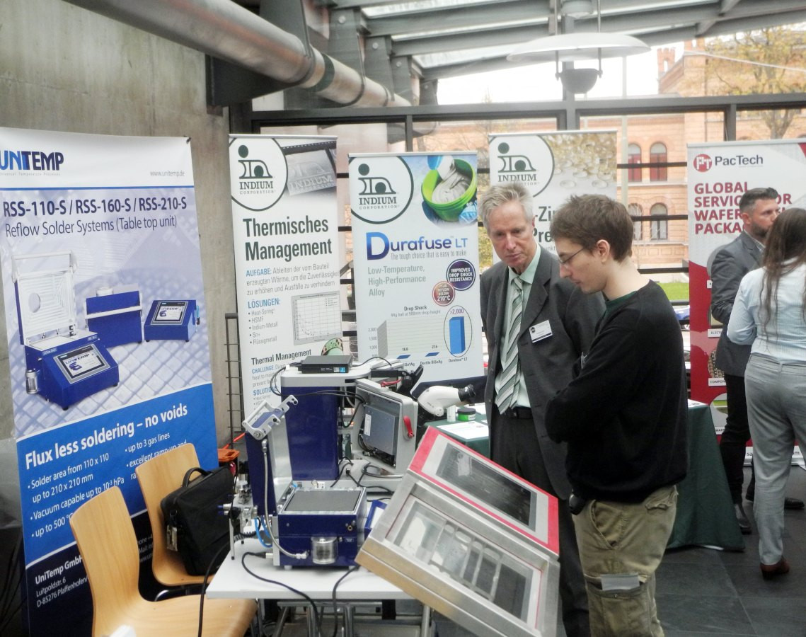
 Prof. Dr. Martin Schneider-Ramelow at the conference openingWithalmost 90 registered participants, 21 speakers and 12 exhibitors, the conference was a success and maintained its reputation as an important exchange platform in the IMAPS community. The opportunity to visit the exhibition during the breaks between presentations encouraged discussions and networking. This year's exhibitors included nanotec, LaserJob, UniTemp, Indium, PacTech, Wachstumskern HIPS, Amadyne, XYZTEC, EKRA, VIA Electronic, budatec and nano-join. Together with the scientific program, the presentation of products and services from the exhibiting companies helped participants to keep up to date with the latest technology and broaden their own horizons.
The 12 presentations on the first day were divided into four thematic blocks: AVT Soldering, Sensors & Actuators, High Frequency Technologies and Reliability & Simulation. We give here a short summary of each presentation, for the deeper insights it is possible to view the presentations on the conference website (see box 'Viewing individual presentations').
The first presentation of the conference was given by Mr. Landulf Skoda (ASP Equipment GmbH). He analyzed the reasons for soldering defects based on theoretical considerations and empirical data and suggested ensuring directional heat dissipation as a possible solution for avoiding defects generated during solder solidification. Directional heat dissipation can be supported by a special pad design or by heat shielding using stencils. The effect of the pad design on the formation of the solidification front was clearly demonstrated.
Gregor Wiedemann from the Brandenburg University of Technology Cottbus-Senftenberg spoke about the extension of SPICE simulation models to include electro-thermal coupling. The comparison of the experimentally determined and simulated states of the circuit components shows clear differences, particularly in the case of electronic modules with significant power losses. The reason for this is the lack of consideration of self-heating in the current SPICE models. Two approaches to adapting the MOSFET models were presented in the lecture and the corresponding simulation results were compared with the experiment. It was shown that the electro-thermally coupled SPICE simulation delivers meaningful results and requires little computing power or time.
 View into the auditorium
 Impressions from the exhibitionLukasAuer from Landshut University of Applied Sciences reported on the results of the tests on low-temperature soldering on printed low-melting polymer substrates. As is often the case with printed electronics, the circuit carriers are produced using screen printing and then fitted with conventional silicon-based components. When using substrate materials with a low melting temperature, isotropic or anisotropic conductive bonding is usually used. The focus of the work was to investigate the solderability of polymer-based silver conductive pastes and to determine suitable solder pastes. The active elements in the QFN housing and the passive SMD components were used for the tests. As a result, suitable combinations of conductive and solder pastes were presented in the lecture.
In his presentation, Prof. Gregor Feiertag (Munich University of Applied Sciences) reported on the challenges of assembly and connection technology for surface acoustic wave filters (SAW) that arise as miniaturization progresses. In the current miniaturization step, the solder balls of a die-size package are replaced by Copper Pillar Bumps (CPB), which reduces the lateral dimension of the contacts and at the same time allows freedom of height adjustment. The presentation will show the process steps necessary for the production of CPBs as well as the results of the extensive reliability tests with the presentation of the typical break points during the temperature shock tests and a detailed analysis of the quality of the soldered connections.
The presentation by Lukas Mennicke from TU Darmstadt was dedicated to a high-precision temperature sensor that can be used in a measuring system for the purity analysis of gases in the ppm range, as required in chip production or the chemical industry. The impurities in gases are determined by detecting the change in molar mass, which in turn can be derived from the speed of sound, temperature and pressure. The measurement is carried out in a system known as a 'fluidistor', in which the speed of sound is measured using ultrasound in an oscillating gas flow. Thanks to its very small thermal mass, the new sensor has a much shorter response time than conventional sensors and enables high-precision measurement.
Corinna Niegisch (Robert Bosch GmbH) has addressed the fundamental question of how the quality of potting in the packaging of electronic components can be improved through a better understanding of the chemical processes that take place during the polymerization of the molding compound. To investigate these processes, a whole series of sensors - pressure, temperature, ultrasound and DEA sensors - are integrated into the molds. The new data, obtained through the additional use of an infrared spectrometer for in-situ measurement, show correlations in the infrared absorption in certain spectral bands and the polymerization state of the molding compound. It is possible to determine the reaction parameters from the measurement data by means of kinetic analysis and to use the knowledge gained for process optimization.
 Lively exchange between the participants during the break
The presentation by Georg Gramlich from KIT dealt with contacting options for packaging MMICs for the frequency range above 100 GHz. Here, wire bonding is to be replaced by printed lines. The suitability of UPD printing technology (Ultraprecise Dispensing) for the creation of such connections was investigated. In UPD printing, an ink filled with nanoparticles is applied via a very thin glass capillary or nozzle; conductor track widths of up to 1.5 µm can be achieved at a printing speed of up to 0.1 mm/s. The gold ink used is sintered for 10 minutes at 250 °C. The high-frequency interconnects shown with widths of 32µm (central line) were successfully realized on aluminium oxide substrates with engraved slots; they exhibit low attenuation and good input matching.
 Treasurer Ernst Eggelaar honoring the sponsors
 Social evening at the Augustiner
Robin Kress from the University of Duisburg-Essen reported on THz components and their integration into modules. The new application areas of THz systems - non-destructive imaging, material detection, extremely broadband communication, biosensor technology - require efficient mobile THz modules that do not yet exist on the market in this form. One of the main challenges for the creation of robust, transportable and easy-to-use modules is the necessary assembly and connection technology. In the lecture, the challenges in the characterization of the components and the steps of the module construction were presented: the integration of the THz source on InP basis and the Si lens by means of bonding processes, flip-chip integration of the THz oscillator on the SiGe CMOS substrate and the construction on FR-4 carriers.
 The speakers of the first and second dayThepresentation by Michael Kaiser (Fraunhofer ITZ, Berlin)alsoaddressed the topic of AVT for next-generation high-frequency modules and components. In this case, the focus was on 6G communication. A high degree of integration is required to handle the signals with the small wavelengths of less than 3 mm that are envisaged. Fan-out wafer level package technology (FoWLP) was proposed and tested as the platform for implementing the modules. The module should contain a front-end RFIC, some rewiring layers (RDL) on PI and the antenna integrated in the package, several modules should be interconnectable to a larger array. In the lecture, the mechanical demonstrators of the integrated structure were presented and the technical difficulties encountered, in particular in the form of warpage, were discussed.
The three presentations in the 'Reliability & Simulation' session were given by doctoral students from Ingolstadt University of Applied Sciences: Nihesh Mohan, Andreas Zippelius and E Liu. Mr. Mohan spoke about the tests and optimizations of the flux-free soldering process and presented the results of the comparison of the reliability of the joints produced with and without flux. Flux residues, as they occur when soldering with traditional reflow pastes, can lead to difficulties, especially with optoelectronic modules. However, flux-free soldering must be carried out in a special atmosphere and can sometimes also lead to the formation of interfering residual substances on the surface, e.g. when formic acid is used as a reducing agent. In the tests, differently housed SMD components were attached to IMS and FR-4 substrates and the solder joints were then examined for quality and reliability.
In the presentation by Andreas Zippelius, the possibilities of using neural networks to predict the reliability of solder joints were presented. For the study, a total of 1800 LEDs of different types were mounted on IMS circuit boards using various solders and subjected to ageing by thermal shock cycling. Using transient thermal analysis (TTA), the changes in the thermal resistance of the solder joint were tracked and the average service life was derived from this. From the data, it was possible to draw conclusions about how the lifetime of the connection is related to the internal structure of the LED. In addition, the measurement data was used to create the neural network capable of predicting the number of component failures during the next stage of thermal aging.
Ms. Liu dedicated her presentation to the investigation of mechanical stress in a bare die component after it has been bonded to a substrate. Both soldered and sintered joints using silver and copper pastes were examined. The mechanical stress in the Si components was measured using µ-Raman spectroscopy on the one hand and simulated on the other. In addition to the theoretical principles presented, which are necessary for the calculation of stresses in the crystal lattice from the Raman shift, experimental results of the planar distribution of the mechanical stress in the component were presented and the reduction of the stress with time was discussed. The dependence of the stress on the thickness of the interconnect layer can be derived from the data.
On the second day of the conference, the results of the first project phase of the HIPS - High Performance Sensors growth core were presented in addition to lectures from the Emerging Technologies topic block.
 The presentation by Daniel Lieske (AEMtec GmbH, Berlin) highlighted the design and manufacturing steps of a chip-scale package. The silicon die originally intended for contacting via wire bonding was redesigned at wafer level by attaching the PI-based rewiring layers and solder balls into a component for flip-chip assembly. In the presentation, the considerations for determining the under-bump metallization were presented and the results of the shear tests on the solder balls for process characterization were shown. The project succeeded in manufacturing the component in a wafer-level chip scale package with high yield.
Silvia Braun from Fraunhofer ENAS spoke about new developments in the thermocompression wafer bonding process. By using aluminum as a metallic layer, it should be possible to reduce the bonding temperature by up to 400 °C. The disadvantage of aluminum, however, is its stable oxide layer, which prevents bonding. The coating of vacuum-deposited aluminum with a palladium layer and the use of an electroplated aluminum layer have been shown as ways of eliminating the effect of the aluminum oxide layer. With the electroplated layer, the roughness of the deposited metal helps to mechanically break through the oxide layer and bring the aluminum layers to be joined into direct contact. As the results suggest, galvanic metallization is more promising and should be pursued further.
Lars Stagun from TU Berlin reported on the integration possibilities of electronics in textile objects. The main focus was on the non-conductive adhesive bonding technology for e-textiles on the special machine developed for this purpose. This makes it possible to connect the rigid circuit board-based electronic modules with the conductor tracks incorporated into the textile. The connection is created by melting a non-conductive thermoplastic adhesive component and can withstand heavy loads, such as those that can occur when the objects are worn or washed. The conductor track can be integrated into the textile carrier by means of several processes, including embroidery, knitting, lamination or even tape-based. The contribution was rounded off with the presentation of some test applications.
 This year's 'Best Presentation Award' went to Mr. Lars Stagun, a research assistant at the TU BerlinMr. Stagun received the 'Best Presentation Award'forhis presentation. Once again this year, many interesting and high-quality presentations were offered to the conference participants, and it was not easy for the board to choose the best one. We would like to take this opportunity to congratulate Mr. Stagun on his award!
In the special session 'Growth Core HIPS - High Performance Sensors', the project results at the end of the funding phase were examined from different perspectives and the underlying SiCer technology (combination of silicon technology with ceramic multilayer technology) and its applications were presented. Knuth Baumgärtel (Micro-Hybrid Electronic GmbH, Hermsdorf) explained the potential of Si-LTCC composite substrates from an industrial perspective, Franz Bechtold (VIA electronic GmbH, Hermsdorf) reported on the current state of development of SiCer technology, the planned next steps and the technical difficulties that are often due to the discontinuation of well-tested materials. Clemens Motzkus from Fraunhofer IKTS in Hermsdorf spoke about the steps taken to scale up the manufacturing process for SiCer-capable LTCC ceramic film. An important milestone was the transition to the continuous film casting process, which allows better material properties to be achieved in terms of basic density, height deviations in the film and drying shrinkage. His colleague Hannes Engelhardt presented the results of the microstructural investigations, in which the reactions in the interface between LTCC and silicon wafer were examined. The realized application examples were presented by Jens Müller (Ilmenau University of Technology) and Andrea Cyriax (CIS Forschungsinstitut für Mikrosensorik GmbH, Erfurt). Mr. Müller spoke about the structure, fluidics and characterization of a sensor module for the investigation of cell cultures using impedance spectroscopy. Ms. Cyriax reported on the successes and challenges associated with SiCer-based packaging of piezoresistive pressure sensors.
In the evening after the first conference day, the conference evening event took place as usual. Traditionally, it was held at Augustiner in Neuhauser Straße, for a change in the white hall, which offered the traditional Munich atmosphere and coziness just as well. During the short speech, the Board of Directors took the opportunity to thank the sponsors of the event: AEMtec, Budatec, EKRA, Hesse, Indium and VIA Electronic. We would like to take this opportunity to thank them once again for their support and contribution to the success of the conference.
Finally, we would like to thank the participants of the conference: Your professional contributions and guided discussions made it a pleasure to be at the conference, as always!
General Assembly of IMAPS Germany on October 20, 2022
The general meeting took place at the end of the first day of the conference. Both the IMAPS members present and the conference participants interested in the work of IMAPS DE e. V. were invited.
In the final report for 2021, the first chairman Prof. Dr. Scheider-Ramelow presented the events of the year and the work of the association. Treasurer Ernst Eggelaar reported on the association's financial situation. After the report, the members of the association approved the actions of the Executive Board.
The election of the second chairman and the treasurer was scheduled. The two incumbent board members - Dr. Stefan Härter and Ernst Eggelaar - were unanimously confirmed in their positions.
The Chairman then reported on the development of membership figures at IMAPS DE and in the other chapters. With 245 active members, the German chapter remains by far the strongest in Europe. In 2022, IMAPS Germany recorded 9 new members and 8 resignations. After the preliminary report for 2022 and the disclosure of the current financial situation, an outlook on next year's events organized or supported by IMAPS was given. The details can be found in the calendar of events.
Viewing individual presentations
To view and download individual presentations, please follow the link https://imaps.de/event/imaps-herbstkonferenz-2022/ and log in via 'Registration'. The individual PDF files are displayed in the list view under 'Event program'
Calendar of events
|
Venue |
Period |
Event name |
Organizer |
|
Ilmenau |
March 23, 2023 |
IMAPS Germany Spring Seminar |
IMAPS DE |
|
Albuquerque |
April 18-20, 2023 |
CICMT 2023 |
IMAPS/ACerS |
|
Oslo |
June 12-14, 2023 |
NordPac 2023 |
IMAPS Nordic |
|
Hinxton |
September 11-14, 2023 |
EMPC 2023 |
IMAPS UK |
|
San Diego |
October 02-05, 2023 |
International Symposium |
IMAPS US |
|
Munich, Germany |
October 19-20, 2023 |
Fall Conference |
IMAPS DE |
|
Munich, Germany |
November 14-17, 2023 |
SEMICON EUROPE |
SEMI Europe |
IMAPS Germany - Your association for packaging and interconnection technology
IMAPS Germany, part of the International Microelectronics and Packaging Society (IMAPS), has been the forum in Germany for all those involved in microelectronics and packaging technology since 1973. With almost 300 members, we essentially pursue three important goals:
- we connect science and practice
- we ensure the exchange of information among our members and
- we represent the position of our members in international committees.
Imprint
IMAPS Germany e. V.
Kleingrötzing 1, D-84494 Neumarkt-St. Veit
1st Chairman: Prof. Dr.-Ing. Martin Schneider-Ramelow, Director of the Fraunhofer Institute for Reliability and Microintegration (IZM),
Treasurer
(for questions about membership and contributions):
Ernst G. M. Eggelaar,
You can find detailed contact information for the members of the Executive Board at www.imaps.de
(Executive Board)
