
Call for Paper for CICMT 2022 - Ceramic Interconnect and Ceramic Microsystems Technologies
Vienna July 13 to 15, 2022
The conference "Ceramic Interconnect and Ceramic Microsystems Technologies" (CICMT) brings together a variety of disciplines. The focus is on sharing experiences and promoting opportunities to accelerate the research, development and application of ceramic interconnect and microsystems technologies. Originally launched by IMAPS North America, the conference has been held at various locations in the USA, Europe and Asia since 2008. After IMAPS Germany has already co-organized the conferences in Munich, Erfurt and Dresden, this year's venue is Vienna.
This international conference offers ceramic technology for both microsystems and interconnect applications in a multi-track technical program.
The Ceramic Interconnect track focuses on cost-effective and reliable high-performance ceramic interconnect products for extreme environments in the automotive, aerospace, lighting, solar and communications industries.
The Ceramic Microsystems track focuses on new applications and new products that utilize the capability of 3D ceramic structures to integrate packaging with microfluidic, optical, microreactor and sensor functions.
 Image: Vienna Tourist Board/Christian Stemper
Multilayer ceramic, thin-film, tape-casting, thick-film hybrid, direct-write and rapid prototyping technologies are common to both tracks, with a focus on materials, processes, prototyping, advanced design and application opportunities. Planned sessions and presentation topics include:
 1. functional materials for passive/active devices and their properties
- Microwave/mm-wave LTCC/ULTCC dielectric materials
- Dielectric/ferroelectric/piezoelectric composites
- Ferroelectric/piezoelectric/pyroelectric/ferrite/multiferroic materials
- Sensitive ceramics/thermoelectric/ electrocaloric materials
- Pastes/inks/slurries for electronics
2. material processing and device manufacturing technologies
- LTCC/HTCC and multilayer ceramic and glass processing
- Emerging ultralow temperature, room temperature processing, and cold sintering processing
- Additive manufacturing /3D printing/ direct writing
- Advanced thick film processing
- Fine structuring technologies
- Emerging embedding/integration technologies
 3. design, modeling, simulation, characterization and reliability

- Metamaterials design, realization and characterization
- High frequency devices design/ modeling/simulation
- Materials and devices characterization
- Material and device reliability, lifetime, and failure estimation
- Thermal management/thermal transfer simulation
4. devices and systems for emerging applications
- Circuits, antennas, and filters for MHz, GHz and THz for communications
- Automotive/aerospace/medical electronics/ optoelectronics
- Flexible/wearable electronics
- Integrated physical/chemical/biological sensors and actuators
- Packaging and integration issues for MEMS and BioMEMS devices
- Batteries/fuel cells/ energy conversion systems
- Micro-reactors/micro-fluidic devices
 Accompanying exhibitionFull papers are due by May 15, 2022 and should be uploaded separately after abstracts have been accepted. All papers will be presented and published in English. In case of problems with the online system, please email the conference office
CICMT 2022 is expected to return as an on-site event. As an exhibitor, you will have the unique opportunity to showcase your products and services to an interested audience of users, developers and influential researchers. Exhibition times are arranged to maximize exhibitor exposure. Coffee breaks are scheduled in the exhibition area to encourage all attendees to meet formally and informally at their convenience. Seating is available on a first-come, first-served basis. We will try to accommodate any special needs and requests you may have.
Details of options and fees will be available shortly.
General Chair:
Ulrich Schmid, TU Vienna
Vice General Chair:
Markus Eberstein, TDK Sensors
Technical Organizing Committee:
- Simon Ang, High Density Electronic Center, University of Arkansas
- Heli Jantunen, University of Oulu
- Eung Soo Kim, Kyonggi University
- Soshu Kirihara, Joining and Welding Research Institute Osaka University
- Daniel Krueger, Honeywell
- Zhifu Liu, Shanghai Institute of Ceramics of the Chinese Academy of Sciences
- Jens Müller, Ilmenau University of Technology
- Uwe Partsch, Fraunhofer IKTS
- Steve Dai, Sandia National Laboratories
- Michael Schneider, TU Vienna
Technical sponsors:
- IMAPS Germany e. V.
- IMAPS International Microelectronics and Packaging Society
- ACerS - American Ceramics Society
Harsh environment interconnection technology for three-dimensional packaging
J. Bickel [1,3], Joachim Scherer [4], M. Schneider Ramelow [2,3], K.-D. Lang [2,3], H.-D. Ngo [1,2]
Ha Duong Ngo can look back on the successful completion of a project on "3D metallization using atmospheric pressure sputtering for harsh environment sensor housings (3D wire)".
A technology was developed that uses atmospheric pressure sputtering to apply thin-film conductors to ceramic blanks for sensor housings in order to create the electrical connection between the sensor and the outside of the housing. The deposited high-temperature metal system was successfully structured using photoelectrochemical etching technology. The first samples demonstrate the flexibility of the process, which enables the ceramic geometry to be adapted to the ambient conditions and the system used.
1. motivation
In the field of SiC electronics, more and more improvements have been made in the area of harsh environment in recent years. Especially in terms of high temperature resistance. While initially only simple transistors were used (P. G. Neudeck, 2008), the first more complex circuits in 6H-SiC are now possible (M. Shakir, 2019). Also in the sector of micromechanical sensors, solutions for temperatures of 500 °C have existed for several years (L. Y. Chen, 2013) (A. A. Ned, 1998). However, the limiting factor today is often the circumstance of reliable and inexpensive interconnection technology (ICT) and packaging technology. Due to the high temperatures and the different CTEs of different materials that are used, only a few raw materials can be considered for high temperature ITC. Obvious materials are ceramics and for low cost systems especially Al2O3. Platinum and gold thin wire bonding is suitable for the interconnect level between chip and substrate (L. Coppola, 2007).
2. state of the art
Since Al2O3, like other ceramics, is difficult to pattern by micro technological methods, the capabilities for ICT are very limited. Thick film pastes of gold and platinum are generally used on planar substrates (R. Zeiser, 2015). The disadvantages are the increased consumption of resources due to the technological and not the physical limits as well as the fact that no through-hole vias or 3D structures can be realized. Today, a punching through hole stud bonding process is often used to establish electrical connections in three dimensions from the chip level to the environment. With such a system, a very large number of steps are required to place the solid metal stud through the hole in the ceramic. Then, layer by layer, the materials have to be stacked on top of each other. Such a stacked system is shown in Figures 1 and 2 and has been used since several years for the application in pressure sensor measuring systems (H. D. Ngo, 2012).
 Fig. 1: Real picture of a common high temperature package. Ceramic carrier from Kyocera
 Fig. 2: X-ray imaging with sensor and bond wires. Three stacked planes are visible
 Fig. 3: Fully automatic production system for 3D APSLD coatings of ceramic blanks
 Fig. 4: Prototype of high temperature pressure sensor packaging produced by using APSLD
3 Technical Approach
To overcome the drawbacks of existing technologies, we have developed a solution that uses the atmospheric pressure sputtering layer deposition technology (APSLD) (J. Bickel, 2019) to enable signal routing on special 3D printed ceramic substrates using platinum and gold metallization. The APSLD technology is used to additively deposit the metal directly and in a structured process in notches that are located along the side of a cylinder. The metal covers only the surface in the notch, as can be seen in Figures 3 and 4. In addition, the metallization coating is applied over the end faces of the cylinder. This allows the ceramic to be subsequently framed and welded as required, including by conductive materials such as Invar or Kovar, and to be contacted from the top and bottom surfaces. Thin-wire wire bonding is very well suited as a contacting solution to the chip level. In this system, SMD solder contacts can be used on the underside, or an FR4 interposer can be attached, as the thermal stress on the underside is no longer in the critical range and since high temperatures no longer exist here.
4 Discussion
Due to the high flexibility of the process, the ceramic geometry can be adapted as required to the environmental conditions and the system used. When applying pure platinum as conductive material, platinum layer thicknesses of 200 to 300 nm can be used for 10 mm long conductors with 10 Ohm resistance and thus technology consumption costs and material costs for the metallization of only a few cents per conductor can be realized. These are significant cost reductions compared to the solid metal connections in today's standard systems. The conductor can be applied fully automatically to any solid material, eliminating the need for further assembly and handling steps for the manufacture of the package itself.
Companies:
[1] University of Applied Sciences, Berlin, Germany
[2] Fraunhofer IZM, Berlin, Germany
[3] Technische Universität Berlin, Berlin, Germany
[4] Aurion Anlagentechnik GmbH, Seligenstadt, Germany
References:
A. A. Ned, R. S. (1998), 6H-SiC pressure sensor operation at 600 °C, Fourth International High Temperature Electronics Conference. HITEC
H.D. Ngo, (2012), Liquid-free SOI-based piezoresistive pressure sensor for measurement up to 400 °C, IEEE Sensors, pp. 100-114, Taiwan
J. Bickel, H.-D. N.-D, (2019), Increasing the productivity of the novel atmospheric pressure sputtering technology for 3D chip interconnection, Pisa: IEEE
L. Coppola, D.H. (2007), Survey on High-Temperature Packaging Materials for SiC-Based Power Electronics Modules, IEEE Power Electronics Specialists Conference
L.Y. Chen, G.W. (2013), Packaging technologies for high temperature electronics and sensors, Joint Conference on 67th Machinery Failure Prevention Technology
M. Shakir, S.H. (2019), Shakir, Muhammad et al, 555-Timer and Comparators Operational at 500 ° C, IEEE Transactions on Electron Devices
P. G. Neudeck, e. a. (2008), 6H-SiC Transistor Integrated Circuits Demonstrating Prolonged Operation at 500 °C, IMAPS HiTEC
R. Zeiser, P. W. (2015), Flip-chip package for pressure sensors with operationtemperatures up to 500 °C, AMA Conferences
In October last year, the IMAPS fall conference was once again held in Munich, as we reported in the December issue. There was also another "Best Presentation Award". The decision was made in favor of the presentation by Kathrin Reinhardt from Fraunhofer IKTS Dresden. Her presentation and the subsequent discussion were convincing thanks to her in-depth knowledge and factual formulation. The presentation was prepared in a very clear and structured manner. She presented a familiar but newly revitalized topic - photostructurable pastes. This could fill the gap between the technically "simple" screen printing process and the technologically complex microstructuring. Ms. Reinhardt has kindly prepared an outline of the topic presented for PLUS.
Photostructurable pastes - the latest innovations in fineline thick-film technology
 Schicht nach Siebdruck, b) Belichtung mittels UV Licht durch eine Negativ-Fotomaske, c) Entwicklung mittels wässriger Lösungen und d) entwickelte Strukturen vor dem Sintern") Fig. 1: Illustration of the two additional process steps: a) layer after screen printing, b) exposure to UV light through a negative photomask, c) development using aqueous solutions and d) developed structures before sinteringDevelopmentsin the field of mobile communication (5G, 6G), (autonomous) mobility and the Internet of Things (smart cities, wearables, object tracking, smart grids, video security) are highly topical in the European research and industrial landscape. This requires ever higher transmission bandwidths and therefore ever higher operating frequencies > 60 GHz. In order to exploit this potential, new technologies are needed to generate the high-frequency circuits, with which ever finer conductor runs with ever closer spacing in the range of 10-30 µm each can be realized. To achieve this goal, Fraunhofer IKTS has developed thick-film pastes that can be photostructured using UV light and can enable the desired geometric resolutions. A comparable technological approach has already been pursued in the past by the company DuPont - FODELTM , but due to a limited variety of materials (gold, silver, dielectrics) and insufficient geometry resolutions (40 µm line widths; 50 µm spacing) it could never be brought to industrial application. In the field of wireless communication, the newly developed IKTS photostructurable pastes (silver, gold, platinum, resistors) therefore represent an enormous added value, which, compared to FODEL, are also more robust (processing under white light), more process-friendly (very short process times) and more environmentally friendly (RoHS/REACH-compatible). For a better understanding, the photostructuring process is outlined in Figure 1. Compared to conventional thick-film technology, two additional steps (exposure and development) are required for structuring after screen printing. The additional process steps only require between 5 and 20 seconds each and can be easily integrated into established production process lines. Exposure can be achieved using either photomasks or maskless laser direct imaging (LDI) processes. This novel feature is made possible by the targeted adaptation of the photosensitive binder and contributes to the digitalization of the process technology and to a further improvement in structural accuracy.
Fig. 1: Illustration of the two additional process steps: a) layer after screen printing, b) exposure to UV light through a negative photomask, c) development using aqueous solutions and d) developed structures before sinteringDevelopmentsin the field of mobile communication (5G, 6G), (autonomous) mobility and the Internet of Things (smart cities, wearables, object tracking, smart grids, video security) are highly topical in the European research and industrial landscape. This requires ever higher transmission bandwidths and therefore ever higher operating frequencies > 60 GHz. In order to exploit this potential, new technologies are needed to generate the high-frequency circuits, with which ever finer conductor runs with ever closer spacing in the range of 10-30 µm each can be realized. To achieve this goal, Fraunhofer IKTS has developed thick-film pastes that can be photostructured using UV light and can enable the desired geometric resolutions. A comparable technological approach has already been pursued in the past by the company DuPont - FODELTM , but due to a limited variety of materials (gold, silver, dielectrics) and insufficient geometry resolutions (40 µm line widths; 50 µm spacing) it could never be brought to industrial application. In the field of wireless communication, the newly developed IKTS photostructurable pastes (silver, gold, platinum, resistors) therefore represent an enormous added value, which, compared to FODEL, are also more robust (processing under white light), more process-friendly (very short process times) and more environmentally friendly (RoHS/REACH-compatible). For a better understanding, the photostructuring process is outlined in Figure 1. Compared to conventional thick-film technology, two additional steps (exposure and development) are required for structuring after screen printing. The additional process steps only require between 5 and 20 seconds each and can be easily integrated into established production process lines. Exposure can be achieved using either photomasks or maskless laser direct imaging (LDI) processes. This novel feature is made possible by the targeted adaptation of the photosensitive binder and contributes to the digitalization of the process technology and to a further improvement in structural accuracy.
|
PI paste on Al2O3 |
Sheet resistance1[ mOhm/sq] |
Burnt layer thickness [µm] |
Line resolution line / distance [µm/µm] |
|
Silver2 (PI1101) |
≤ 3,5 |
8-12 |
20/20 |
|
Gold2 (PI2101) |
≤ 6 |
8-15 |
20/20 |
|
Platinum3 (PI6101) |
≤ 40 |
6-12 |
20/30 |
|
RuO22 (W20024) |
3500 k |
11-17 |
40/35 |
1 Sheet resistivity, calculated for a fired thickness of 10±1 μm
2 Firing profile: 10 min at 850 °C
3 Firing profile: 10 min at 1200 °C
Compared to conventionally printed conductor tracks, the realized cross-sections of the conductor tracks have an almost rectangular shape, whereby the layer thicknesses are sintered in the 8-12 µm range relevant for high-frequency applications(Fig. 2).
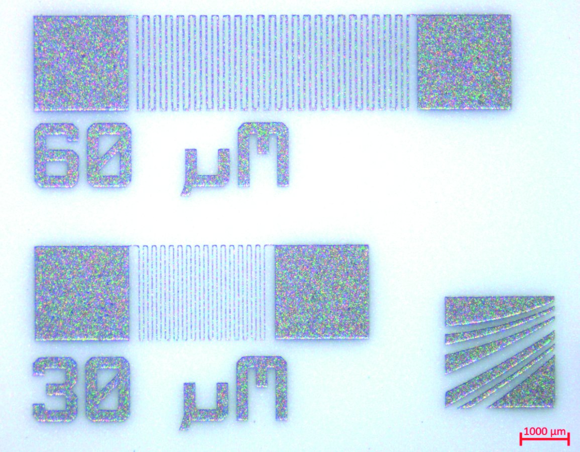
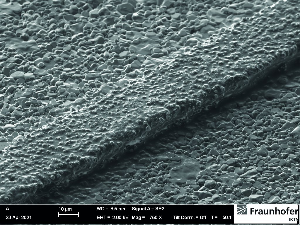
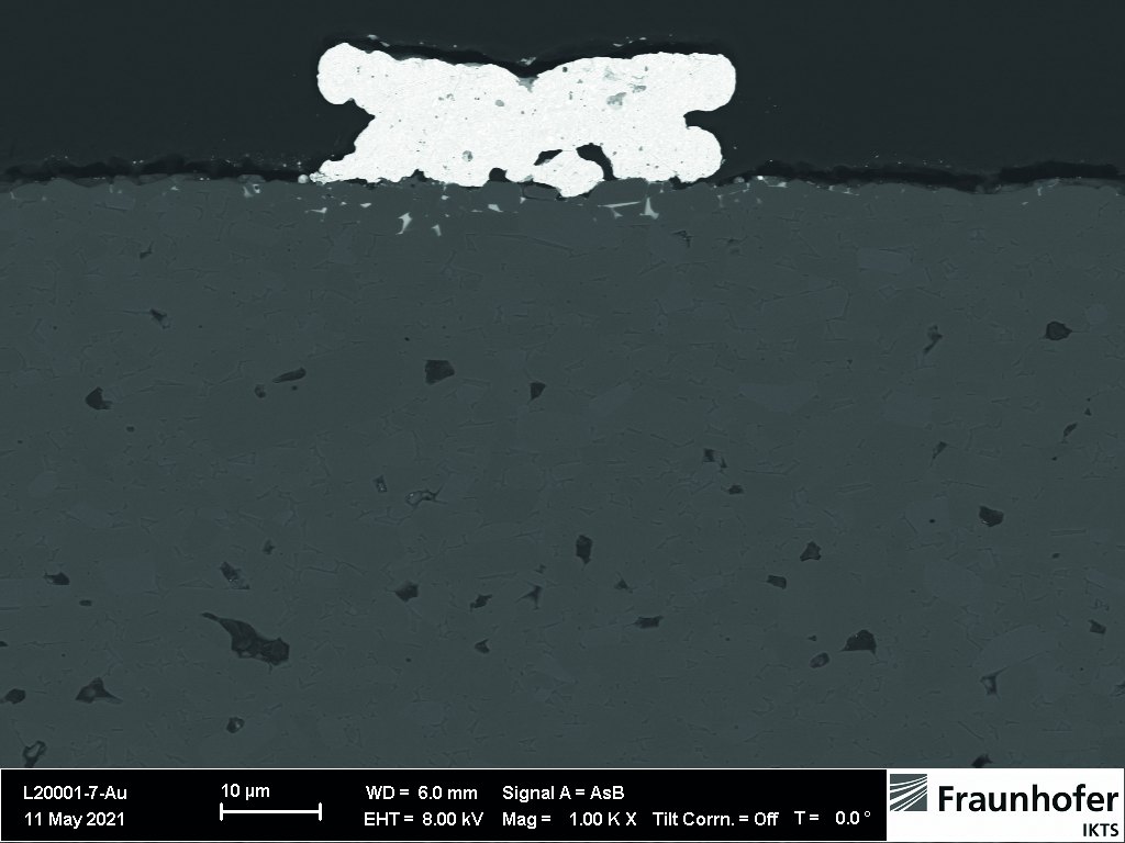
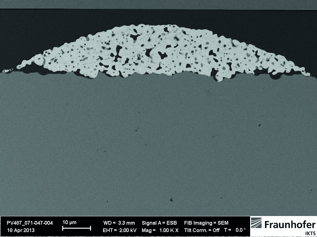
Fig. 2: Structures produced at IKTS using photostructurable pastes with a resolution of 60 and 30 µm lines, each 30 µm apart (top left) and electron micrographs of the unsintered conductor flank (20 µm) (top right), a cross-section of a sintered photostructured (20 µm) (bottom left) and conventionally produced conductor (100 µm) (bottom right).
The focus of current developments in PI pastes at IKTS is on metallization pastes such as silver, gold, platinum and copper. However, PI resistance and dielectric pastes are also currently being developed. Using PI silver pastes as an example, it was shown that these can be used for aluminum oxide substrates as well as for Low Temperature Cofired Ceramics (LTCC). The silver pastes developed thus enable LTCC build-ups in both the post-firing and co-firing process. Line widths of 10 µm and gap widths of 16 µm were realized in the co-sintered state. Initial investigations have also shown that the IKTS-PI pastes are suitable for direct laser exposure. Table 1 summarizes an overview of the properties of the silver, gold, platinum and RuO2 PI pastes with regard to geometric resolution and electrical conductivity on Al2O3 substrates.
The results of the Fraunhofer IKTS PI pastes show a promising mass and industrial process with low investment costs and only slightly higher production time, which can be used to produce components that enable significantly better RF performance at higher frequencies than before and allow significant miniaturization for the future.
IMAPS Germany - Your association for assembly and connection technology
IMAPS Germany, part of the International Microelectronics and Packaging Society (IMAPS), has been the forum in Germany for all those involved in microelectronics and packaging technology since 1973. With almost 300 members, we essentially pursue three important goals:
- we connect science and practice
- we ensure the exchange of information among our members and
- we represent the position of our members in international committees.
Calendar of events
|
Venue |
Period |
Event name |
Organizer |
|
Fellbach |
March 2-3, 2022 |
Electrical assemblies and printed circuit boards EBL 2022 |
DVS / GMM |
|
Fountain Hills, AZ |
March 7-10, 2022 |
Device Packaging Conference |
IMAPS US |
|
Grenoble, FR |
March 10-11, 2022 |
MiNaPad 2022 |
IMAPS France |
|
Landshut |
April 6, 2022 |
Symposium Electronics and System Integration |
HS Landshut |
|
Gothenburg, S |
June 12-14, 2022 |
NordPac 2022 |
IMAPS Nordic |
|
Vienna, AT |
July 13-15, 2022 |
CICMT 2022 |
IMAPS |
|
Sibiu, RO |
September 13-16, 2022 |
ESTC 2022 |
IEEE-CPMT IMAPS Europe IEEE-CPMT IMAPS Europe |
|
Berlin |
Sept. 26-29, 2022 |
ESREF 2022 |
IZM / TU |
|
Boston, MA |
October 3-6, 2022 |
International Symposium |
IMAPS US |
|
Munich, Germany |
Oct. 2022 |
Fall Conference |
IMAPS D |
|
Munich, Germany |
Nov. 2022 |
SEMICON EUROPE |
SEMI Europe |
Imprint
IMAPS Germany e. V.
Kleingrötzing 1
D-84494 Neumarkt-St. Veit
1st Chairman:
Prof. Dr.-Ing. Martin Schneider-Ramelow,
Deputy Director of the Fraunhofer Institute for Reliability and Microintegration (IZM),
Treasurer
(for questions about membership and contributions):
Ernst G. M. Eggelaar,
You can find detailed contact information for the board members at www.imaps.de
(Board of Directors)
