Electronic assemblies and printed circuit boards, EBL
11th DVS/GMM Conference
From 14.06. to 15.06.2022, the 11th DVS/GMM Conference will open its doors in the Schwabenhalle Fellbach. Under the motto "Electronic assemblies and printed circuit boards - intelligent design, intelligent production, testing and applications", visitors can once again expect current lectures on the topic of "Data - curse or blessing", which will be accompanied by an exhibition of 21 exhibiting companies and associations. iMAPS-Deutschland e. V. is also supporting this event with numerous specialist lectures and various members who will be presenting their products and services to the specialist audience during the accompanying exhibition.
Keywords such as "data mining, cloud solutions, artificial intelligence, augmented and virtual reality" are now an integral part of the age of digital development. Data is generated starting with the development and design of new products, during the production of prototypes, engineering samples and industrialization, during series production and in in-process quality control. Increasing digitalization makes it possible to record, collect and evaluate these data volumes.
But what do we do with this data? Bernd Enser, Chairman of the Program Committee, and Prof. Dr. Mathias Nowottnick, Scientific Conference Director, answer this question as follows:
"Research has made great progress and, with its specialized knowledge, enables the understanding of many phenomena and the targeted development of new solutions. Some generalists also have a good overview of the interrelationships of the entire process chain. However, the evaluation of this wealth of information in all its breadth and depth requires the support of artificial intelligence, which is able to detect typical patterns and previously unknown relationships from this data. AI has neither imagination nor problem awareness, not to mention moral and ethical considerations. What is needed here is human intelligence, which in the best case scenario cooperates with artificial intelligence.
Current discussions show us just how important this awareness of the problem is. For example, the extraction of raw materials for electronic components and assemblies should meet minimum ecological and humanitarian standards. Strategically important technologies must also be available in Europe, as the pandemic has made us realize. Industry 4.0 has already harmonized the work processes of man and machine so that people can benefit from this cooperation. Similarly, information processing between humans and computers must also be harmonized in order to optimize the efficient and sustainable production of innovative and reliable products. It is therefore essential that users and users understand the system, recognize opportunities, but also get to know the possibilities for concrete implementation."
The main topics of the conference will be
- Intelligent system concepts, design tools and simulation
- New materials, sustainability
- Functional and circuit carriers
- Module and assembly production
- Innovative construction methods
- AVT (soft soldering, etc.)
- Process simulation and control
- Traceability, compliance, product and process safety
- Reliability and analytics
- Corrosion and migration
- Trends, roadmaps, sustainability
- Industry 4.0 / Machine
- learning
|
The entire program can already be viewed today at https://www.ebl-fellbach.de |
Once again, a special highlight of the event will be the presentation of the EBL Prize for Young Scientists. In a special session on the first day of the conference, the best work in the field of industry-related research in the field of packaging technology will be awarded a certificate and prize money for further developments or innovations. We are already looking forward to exciting presentations.
iMAPS e. V., Matthias Lorenz, Public Relations
Detecting THT problem areas at an early stage - model-based design for manufacturing in selective wave soldering
Reinhardt Seidel and Jörg Franke
Chair of Manufacturing Automation and Production Systems (FAPS),
Friedrich-Alexander-University Erlangen-Nuremberg, Nuremberg
Summary
THT solder joints repeatedly lead to production problems because the required solder penetration cannot be achieved. In order to get such problems under control, meaningful models are required that can quantify the solder penetration already at the design stage. The following article presents the approaches developed in the AIF IGF project Siwolak [1] for calculating the solder penetration.
Introduction and motivation
Wave and selective wave soldering are reliable, inexpensive and widely used soldering processes for the automated soft soldering of THT components. The so far not quantitatively assessable soft solderability in terms of the thermal feasibility of a solder joint regularly leads to problematic solder joints in production. Thick copper layers and thermally solid components are particularly required in electromobility and renewable energy applications. However, if the copper layer design is unsuitable, this increases the soldering heat requirement via the soldering heat supply through the selective wave. This results in longer design phases for companies, damage due to error costs, increased production costs, reduced quality and, as a result, reduced competitiveness. Compliance with company-internal, empirically based design guidelines, for example, is only suitable for alleviating the problem to a limited extent, as the heat requirement cannot be quantified in this way.
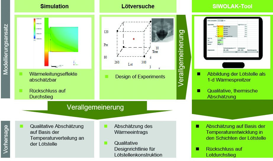
 Fig. 1: Procedure for developing a model for predicting solder penetration
To address this problem, the selective soldering process was investigated using statistical test plans and simulation models and compared iteratively (see Fig. 1). With the aim of identifying thermally critical solder joints early in the design process and determining computer-aided soldering parameters, an Excel tool was developed based on the findings. This model takes into account the main process influencing factors, the thermal properties of the component and the copper layer structure at each solder joint. It can therefore be used to support the development process.
Deriving design recommendations from experimental and numerical studies
The implementation of a multiphysics CFD model using ANSYS-Fluent allows the consideration of the solder gap current as a capillary current using the Volume of Fluid (VOF) method in a parameterized configurable solder joint. This also enables good quantitative predictions to be made. However, the prediction process requires a lot of computing time. For the 2D model, approx. 1h/soldering second must be applied, for the 3D model approx. 24h/soldering second.
 Fig. 2: Validation of the simulation results using soldering tests
Statistical test plans were carried out for the experimental and simulative investigation of the selective wave soldering process and the design variants. In the test procedure, each solder joint is soldered individually. This ensures reproducible boundary conditions for the soldering and influences of the solder joint design are not superimposed by the soldering sequence. The influences investigated included typical component types used in through-hole technology such as connector pin, film capacitor (Foko), electrolytic capacitor (Elko) and metal-oxide semiconductor field-effect transistor (Mosfet). The contact design was discretely differentiated by the number, thickness and connection of layers as well as the hole gap and heat traps in order to be able to make detailed statements about the respective design situations. The investigated process window ranges from 260 °C to 300 °C solder temperature.
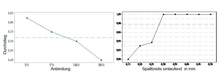
 Fig. 3: Experimental results of the influence of the layer structures (left) and circumferential gap width on the solder penetration (right)
The influence of the layer structure was particularly investigated in the studies. In particular, the layer thickness and the location of the contact play an important role here, as already introduced above. Figure 3 shows the influence of a bond on top (T) and top and bottom (TB) for 35 and 70 µm. It also shows that two thinner layers (TB35) have a slightly lower step-through than one thicker layer (T70). The influence of the circumferential gap width between hole and pin also shows an important influence on the solder penetration when averaged over different contacting designs. With regard to the hole diameter, the larger the hole, the better the solder penetration.
Standardized to the PCB thickness, this results in a gap ratio ratio Equation <1> of approx. 35 to 40 % from which the design influence decreases during selective wave soldering. The reason for this is that as the aspect ratio of hole diameter to PCB thickness increases, the flux penetration and the energy introduced by the greater solder mass flow is improved. Flux penetration in particular plays an important role for thicker PCBs, as the aspect ratio quickly deteriorates if the gap width remains the same.
With regard to the solder joint design, sufficient clearance must be ensured on the solder source side, especially for thermally demanding solder joints with solid copper connections, component pins with high thermal capacity and/or large copper cross-sections on the solder target side, and some basic recommendations can be made from the extensive statistical test plans and CFD simulation studies. Until quasi-thermal equilibrium is reached, the temperature of the solder joint increases exponentially with saturation. The influence of the solder contact time is not statistically significant from the quasi-thermal equilibrium of a solder joint. The influence of the nozzle diameter is sometimes considerable. Larger nozzle diameters introduce more heat over the larger surface area, which leads to significantly improved solder penetration. The soldering tests show that the simultaneous soldering of all component pins leads to a significant improvement in solder penetration. This is due to the simultaneous heating of several vertical through-hole metallizations in the PCB, which reduces the anisotropy of the heat conduction of the copper FR4 layer structure and heats the component on all pins. This also reduces the influence of the component's thermal capacity.
For wave soldering, [2] recommends a gap ratio (Eq. 1) of 15 to 20 %. For selective wave soldering, a value of 35 to 40 % is recommended from the test series.
With regard to the connection of a copper layer to the through-hole metallization, care should be taken to attach solid copper layers only on the solder source side of the PCB. Connections on the inside or on the solder target side must be provided with heat traps and/or thermal vias, especially for thicker layers (from 70 µm depending on the situation) and for components with high thermal capacity.
Siwolak tool
To calculate the overall process in a model, the component and the layer structure must be mapped together with the process conditions. To do this, the thermal properties of the component pin and the layer structure in the solder joint must be modeled. Thermal equivalent circuit diagrams are defined for this purpose. By appropriately parameterizing these equivalent circuit diagrams, different components and solder joints and their behaviour in the soldering process can be mapped.
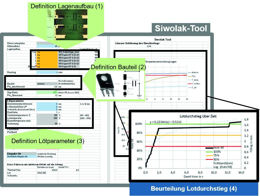
A model proposed by Klein-Wassink in [3] is used for the component. The thermal capacitance of the pin and the thermal resistance in the component body are neglected. To model different layer structures, the copper layers and their connection to the through-hole metallization are characterized layer by layer according to thermal resistance and thermal capacitance. The multi-layer structure is then reassembled into an overall structure so that the bottom layer heats the layer above it. This allows the successive heating of the layer structure to be estimated. Assuming that the solder in the solder gap rises to the point at which it falls below the solder melting temperature, it is possible to assess the progression of the solder rise over time as a function of the layer build-up, as illustrated in Figure 4.
 Fig. 4: Control panel of the Siwolak tool with definition of the layer structure with up to 6 layers, selection of the component, definition of the soldering parameters and result plot of the solder penetration
The validation of the model using soldering test data shows an average deviation of 20 to 30 % between the soldering test and the analytical prediction. In view of the fact that the standard deviation in the process is in the range of 5-15 % and the assessment of the solder penetration is based on manual optical or X-ray inspection, the tool is an aid to quantitative assessment and identification of thermally critical solder joints despite the deviation.
Summary and outlook
The selective wave soldering process is a widely used soldering process in mixed-material printed circuit boards. The soldering process must be regarded as critical with regard to the overall process of printed circuit board production, as the soldering quality is significantly influenced by the solder joint design. The results obtained illustrate the potential of using models in PCB development to reduce design loops, production problems and rejects.
Further promising projects for the automated evaluation of interconnected PCB designs in an overall context with the aid of machine learning methods are currently in the application phase. If you have any questions, please do not hesitate to contact the author at the e-mail address provided.
Bibliography
[1] Seidel, R.; Franke, J.: THT-Problemstellen frühzeitig erkennen - Simulative und experimentelle Untersuchung des Selektivwellenlötprozesses, In: Schweißen und Schneiden, Düsseldorf: DVS Media GmbH, 2021, pp. 772-777
[2] Chang, S.; Wang, R.; Xiang, Y.; Wang, P.; Shi, W.: Design for manufacturability of PTH solder fill in thick board with OSP finish, In: 2011 12th International Conference on Electronic Packaging Technology and High Density Packaging: IEEE, August 8-11, 2011, pp. 1-8
[3] Klein Wassink, R. J.: Soldering in Electronics, 2nd ed., Leuze Verlag, Bad Saulgau, 1991
IMAPS Germany - Your association for assembly and connection technology
IMAPS Germany, part of the "International Microelectronics and Packaging Society" (IMAPS), has been the forum in Germany for all those involved in microelectronics and packaging technology since 1973. With almost 300 members, we essentially pursue three important goals:
- we connect science and practice
- we ensure the exchange of information among our members and
- we represent the point of view of our members in international committees.
Imprint
IMAPS Germany e. V. Kleingrötzing 1 D-84494 Neumarkt-St. Veit
1st Chairman: Prof. Dr.-Ing. Martin Schneider-Ramelow, Director of the Fraunhofer Institute for Reliability and Microintegration (IZM),
Treasurer (for questions about membership and contributions): Ernst G. M. Eggelaar,
You can find detailed contact information for the board members at www.imaps.de
(Board of Directors)
Calendar of events
|
Venue |
Period |
Event name |
Organizer |
|
Landshut |
April 6, 2022 |
Symposium Electronics and System Integration |
HS Landshut |
|
Gothenburg, SE |
June 12-14, 2022 |
NordPac 2022 |
IMAPS Nordic |
|
Grenoble, FR |
June 23-24, 2022 |
MiNaPad 2022 |
IMAPS France |
|
Vienna, AT |
July 13-15, 2022 |
CICMT 2022 |
IMAPS |
|
Sibiu, RO |
Sept. 13-16, 2022 |
ESTC 2022 |
IEEE-CPMT, IMAPS Europe IMAPS Europe IEEE-CPMT |


