Using embedding technology, researchers at Fraunhofer IAF have integrated their monolithically integrated GaN power ICs as a half-bridge circuit including gate and DC link capacitors on PCB material. This provides an extremely compact, efficient and highly integrated voltage converter in the 600 volt class in an application-friendly design for power electronics applications. It is extremely resource-efficient and can be used in a modular fashion.
 X-ray image of the half-bridge circuit and circuit diagram of the integrated GaN power ICs Power semiconductors have been used in voltage converters for years in order to meet the increasing demands on energy supply and utilization and to develop the necessary system components. However, it is not only the semiconductor materials that are important, but also the structure and design of the components: the more compact and efficient the structure, the more resource-efficient the components are.
However, with the discrete standard components that dominate the GaN power electronics market, it is often difficult to achieve the required compact system design. Until now, the critical conductor loops between transistors and the power supply have had to be individually constructed and wired as circuits from discrete components.
"Although GaN-on-Si technology enables monolithic integrated circuits ... but does not solve the wiring problem ..."
The Fraunhofer Institute for Applied Solid State Physics IAF in Freiburg is one of the world's leading research institutes in the fields of III/V semiconductors and synthetic diamond. It has developed the user-friendly, highly integrated GaN voltage converter in order to better support the future requirements of energy-efficient power electronics for energy conversion and transmission, for example in electromobility or power supply from renewable energies. Thanks to the integrated functionality in the chip and all critical, passive components on the housing, the component can be used in a modular way and thus reduces the effort for the development of power electronic systems of the future.
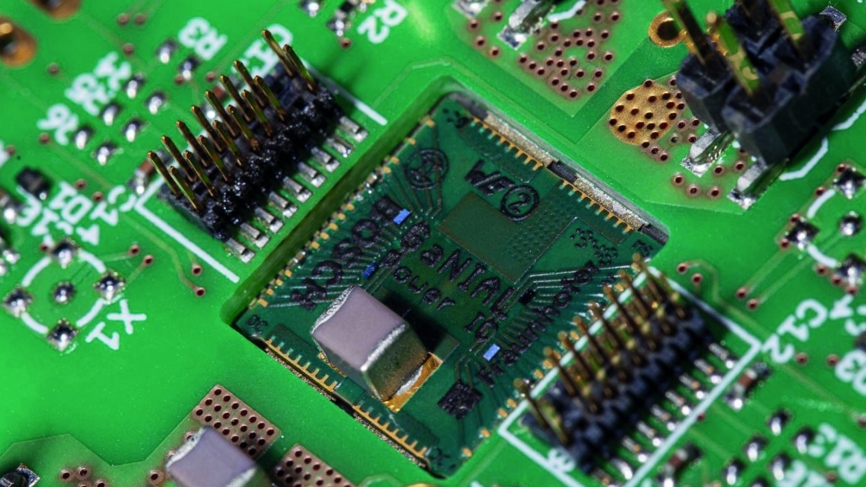
The researchers at Fraunhofer IAF have embedded their gallium nitride-based integrated power circuits (GaN power ICs) as a half-bridge in a small printed circuit board, which at the same time already provides the critical wiring including gate and DC link capacitor as a housing. The resulting voltage converter is highly compact and efficient. It is suitable for all 600-volt applications and enables a reliable modular system design. Design and production processes are significantly simplified.
IAF presented its latest GaN power electronics at PCIM, which this year took place in digital form as 'PCIM Europe digital days' from July 7 to 8, 2020. Fraunhofer IAF's GaN Power IC is also part of a presentation by Dominik Koch (University of Stuttgart) at the accompanying PCIM Europe conference.
Monolithic integrated GaN power ICs
Fraunhofer IAF has many years of experience in the monolithic integration of power electronic GaN chip technologies. Last year, as part of the GaNIAL research project, the Freiburg researchers already succeeded in monolithically integrating current and temperature sensors, 600 V-class power transistors, intrinsic freewheeling diodes and gate drivers in a single GaN power IC. The semiconductor material gallium nitride was deposited on an inexpensive silicon substrate (GaN-on-Si), making the chip technology suitable for cost-effective use in mass applications and in industry.
Thanks to the high integration density, the GaN Power IC from Fraunhofer IAF not only enables a higher switching frequency and thus a higher power density than comparable circuits, but also increased reliability and compactness due to the integrated sensor technology. With the GaN Power ICs in a half-bridge circuit, the researchers have already achieved DC-DC efficiencies of over 98.8 % at 350 V and demonstrated a high switching frequency of 40 MHz in continuous operation at 250 V and resonant operation.
Highly integrated through PCB embedding
"Although GaN-on-Si technology enables monolithic integrated circuits for half-bridge converters, it does not solve the problem of wiring to external capacitors. However, these critical connections to the gate driver and DC link voltage are essential for clean and efficient switching behavior. To get closer to our goal of an optimal voltage converter, the next step was to find the perfect highly integrated packaging technology for our GaN power ICs," explains Stefan Mönch, scientist at Fraunhofer IAF. To this end, they processed their ICs with a thick copper electroplating on both sides, making them suitable for embedding in a printed circuit board (PCB).
This adaptation of the metallization enabled Würth Elektronik CBT to build the chips using the reliable ET Microvia embedding technology, which is suitable for series production. Together with the project partners Bosch and the University of Stuttgart, the researchers were able to design a PCB housing that is only 12 mm wide and 0.4 mm flat, integrating two monolithic GaN power ICs as a half-bridge and providing the critical decoupling capacitances for the gate driver and DC link voltage on the housing. The embedding technology eliminates the need for bonding wires, which also minimizes parasitic inductances. The critical connections between the GaN IC and the capacitors are therefore already optimized and no longer need to be elaborately designed by the user. The result is a user-friendly solution that provides all critical components of a switching converter already optimized in one housing.
Fraunhofer IAF develops components for electronic circuits in the field of communication and mobility solutions, laser systems for spectroscopic real-time sensor technology, novel hardware components for quantum computers and quantum sensors for industrial applications. With its research and development work, the Freiburg research institute covers the entire value chain - from materials research, design and processing through to the realization of modules, systems and demonstrators.
