There are indications worldwide that artificial intelligence (AI) is being used to raise the electronics industry to a new level of quality, either in part or as a whole. A striking example for the development of super ICs, complex semiconductor modules such as SoCs and PCBs is the DARPA project IDEA.
Parts 1 and 2 of this report outline the revolutionary goals of IDEA. Part 3 presents other European and American projects to embed AI in the design and production of printed circuit boards.
IDEA + POSH + 27 other projects = ERI
In addition to IDEA, the associated POSH (posh Open Source Hardware) project must also be mentioned. This aims to create a Linux-based platform and an ecosystem for designing and verifying open source IP hardware blocks for next-generation system-on-chip ICs. Both projects and 27 others are part of ERI, the Electronic Resurgence Initiative launched by Darpa in 2017 [3]. Literally translated, this means 'Electronic Resurgence Initiative'. It was launched not only to revive the domestic chip industry in the USA, which has been increasingly relocated to Asia for decades, but also to raise it to a new level in general under the banner of the future of microelectronics. But something else seems to have startled the DoD: China is pouring huge sums of money into building and expanding its chip industry and has declared that it wants to make chips that add AI to every device. This is a clear global target for the electronics of the future.
IDEA and POSH are actually part of a complex of five topics that are summarized at ERI under the title 'Mitigating the skyrocketing costs of electronic design'. The remaining three topics are
- Common strategies for heterogeneous integration and reuse of intellectual property (IP) (CHIPS)
- Real-time machine learning (RTML)
- Intelligent automatic generation and composition of surrogate models (DITTO) (AIE)
The vulnerabilities in the supply chains of the global electronics industry revealed by the corona pandemic have given the DARPA efforts of 2017 even greater urgency, especially since the future of Moore's Law is also uncertain and the much larger complex IC systems of the future will have to be realized using SoC or chiplet technology for both technological and economic reasons.
In [4] there is a somewhat more precisely formulated justification for the start of ERI (and thus of IDEA and POSH), which should also be reproduced here as a supplement.
The projects within ERI are intended to accelerate the development of complex, highly individualized SoCs. ERI is motivated by two trends in chip design: First, because the roadmap for Moore's Law is slowing, SoC designers are less dependent on CPUs and more dependent on a growing necessary abundance of GPUs, FPGAs, neural chips and other co-processors, increasing the electrical as well as physical complexity of the circuit systems required. Secondly, the experts see a greater variety of applications for the aforementioned semiconductor components, ranging from cloud-based AI to software-defined networks and the Internet of Things. Such diverse applications often require very different processor mixes, including novel chips such as accelerators for neural networks. Here, too, a necessary extensive modular system of different circuit components emerges, which must be 'assembled' as efficiently as possible into finished systems of the highest complexity in the shortest possible time.
It continues in [4]:
Darpa envisions the technology world moving toward a greater variety of SoCs with different mixes of IP blocks, including highly customized SoCs for specific applications. However, with today's semiconductor design tools, such a scenario would be mired in rising costs and delays. ERI plans to speed things up.
The EDA project IDEA as part of ERI is mainly based on the work of David White at Cadence. The immediate goal is to develop a layout generator that will allow users with even limited electronics design experience to complete the physical design of electronic hardware such as a single board computer within 24 hours. A larger goal and also a fundamental requirement for IDEA and thus also ERI is to enable the automated EDA system to capture the know-how of the designers who use it in order to process it automatically, so that it is effectively available as a system-carrying AI in the background for the design work.
Goal: total design automation
On September 22, 2017, the first Proposers Day for IDEA and POSH took place in Mountin View, California [5]. ERI is explained in detail in the 89-slide basic document of the event, which is to be regarded as the intellectual basis of the meeting and also of the project itself. The statistical overview in Figure 3 demonstrates the widespread interest in ERI, IDEA and POSH. The time horizon for the first stage of implementation was boldly set at 2018-2023.
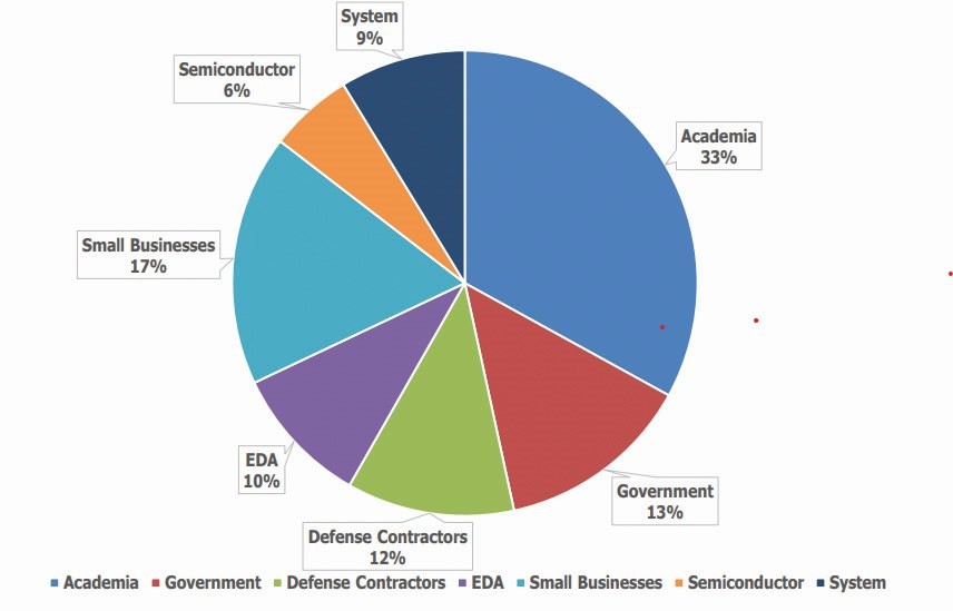 Fig. 3: Broad interest in ERI at the Proposers Day in September 2017
The participants' discussion was based on IDEA's goal of creating a turnaround layout generator that is able to complete the design documents for system-on-chips, system-in-packages and printed circuit boards within 24 hours without human involvement ('no human in the loop'). The following is a small selection of slides from the basic document, which is intended to convey the basic aspects of IDEA. The many other slides deal with more specific details on ERI as well as IDEA and POSH, which would exceed the aim and scope of this article.
 Fig. 4: IDEA covers all four stages in the creation of electronics: chips, chip modules, printed circuit boards or finished assemblies, final devices in the housing
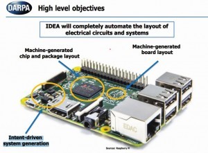
Figure 4 outlines the scope of what is expected from IDEA. The question is: Can manual labor be replaced by machines? According to Figure 5, IDEA should fully automate the layout of electrical circuits and systems:
- Intention-oriented system generation
- Machine-generated chip and package layout
- Machine-generated board layout
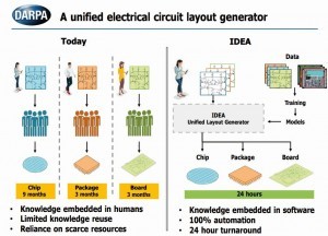
The aim is to transfer the knowledge of system, circuit, chip and board developers to the IDEA Unified Layout Generator (standardized layout generator) by means of training via models(Fig. 6). The basis of the system is therefore
- Knowledge embedded in software
- 100 % automation
- 24-hour processing time specifications
The following factors(Fig. 6) are a brake on the significant acceleration required to create new, highly complex electronic systems:
- Knowledge embedded in people
- Limited reuse of knowledge
- Dependence on scarce resources
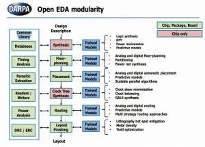
The ultimate goal is open EDA modularity and a standardized design flow as shown in Figure 7. The green process steps are basically the same for chips, chip modules and printed circuit boards. A common standardized library serves as the basis.
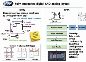
The aim is to achieve a fully automated digital and analog layout. Today, according to the basic document, the developer still makes manual design specifications (constraints) to the layout designer or the CAD system. In future, the layout constraints are to be created automatically by classifying the circuit diagram (circuit patterns) on the basis of certain strategy specifications from the knowledge database(Fig. 8).
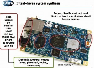
IDEA is based on intent-driven system synthesis(Fig. 9). The aim is to specify what needs to be done and not how. The latter is the task of the system. The board specifications should be very minimal. Example specifications: 5V, Ethernet, USB, HDMI, 1GB RAM, 128 MB Flash, FPGPA, 20 GFLOPS, ARM A9.
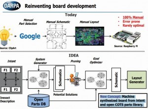
Figure 10 once again demonstrates the differences between the previous way of working (100% manual, error-prone, rarely optimal) and the new approach (machine-synthesized board based on the intention specifications and on the COTS parts library). The solution is to reinvent board development.
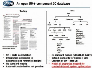
Figure 11 shows the situation of today's component base:
- More than 5 million components in circulation
- The information is embedded in datasheets and reference designs
- No standard models
- Automatic optimization not possible
This is to be contrasted with a different approach in IDEA:
- IC standard models (LEF, LIB, IP-XACT)
- Extend standards for boards/SIPs
- Creation of a comprehensive 5M+ parts database
- Modeling of all required properties for constraint-based system optimization
Project details are described in the many other slides. ERI is mainly about faster, more effective and safer development of new electronics, which in itself would be a huge step forward. Now imagine that the digitally available production data is immediately transferred to the production of a network of smart factories using 5G or 6G data networks as part of Industry 4.0. The overall effect for the electronics industry and thus also for the economy would be immeasurably greater. It can be assumed that Darpa has already considered this conceptual or strategic bridge-building. The question is to what extent the large and, in particular, small manufacturing companies are willing or able to accept such new procedures and forms of organization.
Project process to date
Companies and institutions were able to submit applications to participate in IDEA with corresponding service offers to Darpa by the end of January 2018. It is interesting to note that Serge Leef has taken over the project management for IDEA at the DoD institution. Leef is regarded as an experienced EDA expert who moved to Darpa following the takeover of Mentor Graphics by Siemens. Why do you think?
In June 2018, ERI launched OpenROAD (Foundations and Realization of Open, Accessible Design), another project aimed at helping to successfully implement IDEA.
The overall Darpa-ERI meeting took place in San Francisco in July 2018. Cadence's involvement in IDEA was also confirmed by Darpa. IBM, Intel, Nvidia, Qualcomm and other companies had already done so.
To fulfill the program charter during the four-year term of its contract, Cadence has launched the MAGESTIC (Machine Learning-driven Automatic Generation of Electronic Systems through Intelligent Collaboration) research and development program. This program aims to increase system design performance by introducing greater autonomy within the design process and developing truly design-driven products. The team led by Cadence includes Carnegie Mellon University and NVIDIA, two of the most renowned machine learning leaders in the world [4].
During the overall ERI meeting in 2018, Darpa also announced the first funding for the ERI projects. In a first round, an initial $1.5 billion was announced for the next five years. Cadence was the first to receive a grant of 24.1 million dollars for IDEA.
The Darpa-ERI Summit 2019 took place in Detroit in mid-July. A session section on IDEA focused on the sub-project 'MAGICAL: Machine Generated Analog IC Layout'. A research team from the University of Texas (Austin) presented their work progress for discussion. It is noteworthy that the 8-member MAGICAL research group consisted exclusively of people of Chinese origin, from the professors to the doctoral students and research assistants. In another session section, the topic of 'Generative User-Intent Design of Electronics' was discussed under the leadership of Northroop Grumman.
The Darpa-ERI Summit 2020 was organized for August in Seattle despite Corona. This underlines the urgency of the project from a government perspective. The Darpa-ERI Summit 2021 has been announced as a virtual event for October 19/21 [3]. All poster presentations and other material for the three summits held to date are freely downloadable from the website listed in [3].
Looking to the near future
If one mentally combines the ongoing massive plans of the US government to build numerous new chip factories in the USA for the lower nanometer range from 28 to 5nm with the huge ERI project, one can assume that a kind of "electronics revolution" could take place in the USA in the coming years - if ERI can actually be implemented in parallel. Although IDEA is primarily a military project, it can be assumed that the positive results will also be used for the civilian side, as is usual in the USA. If the IPC's CFX (Connected Factory Initiative) is added to this, more and more foundations are being laid in the USA for a new quality electronics industry. The IPC-2591 standard enables 'plug-and-play' IoT communication throughout the manufacturing environment, where all devices, manufacturing processes and transaction stations can communicate without special software. Version 1.3 from February 2021 is currently valid. This standard is also being systematically developed for Industry 4.0 and the smart factory. The list of companies that support CFX is constantly growing [6].
In the following part 3 of this article, further European and American projects are presented in which attempts are being made to anchor AI in the design and production of printed circuit boards.
References
[1] https://de.wikipedia.org/wiki/K%C3%BCnstliche_Intelligenz#Begriffsherkunft_und_Definitionsversuche
[2] www.darpa.mil/program/intelligent-design-of-electronic-assets
[3] https://eri-summit.darpa.mil/
[4] www.linux.com/topic/embedded-iot/darpa-drops-35-million-posh-open-source-hardware-project/
[5] www.darpa.mil/attachments/eri_design_proposers_day.pdf
[6] www.ipc.org/cfx-supporters


