When testing and commissioning printed circuit boards manually, augmented reality can help to significantly simplify the work and make it easier to detect errors. Previously, when measuring PCBs, it was always necessary to switch between different views of a circuit diagram, a description of the pin assignment of more complex components, data sheets and the prototype.
For fine-pitch components with small distances between the pins, meticulously counting down to the pin to be measured is prone to error. With the inspectAR overlay viewer, the commissioning of PCBs is revolutionized by augmented reality.
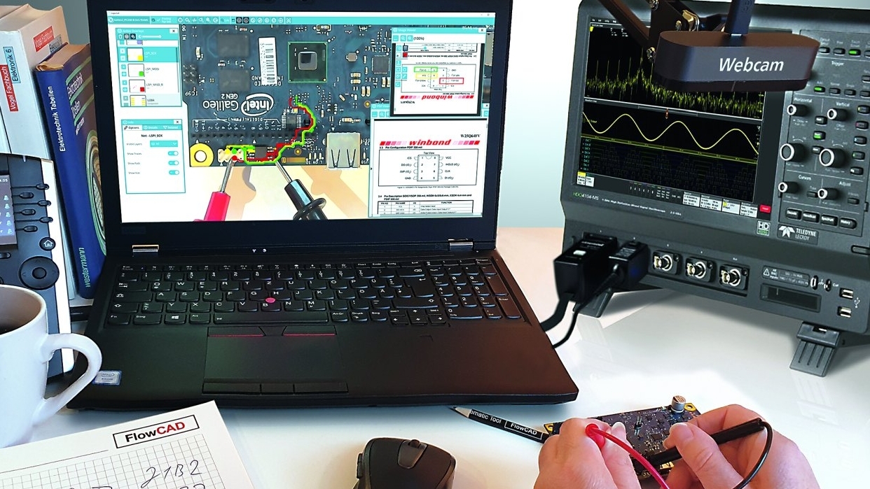
Augmented reality is the computer-aided expansion of the perception of reality through the visual representation of information, i.e. the supplementation of images or videos with computer-generated additional information or virtual objects by means of overlay or superimposition. The PCB overlay viewer inspectAR uses this augmented reality technology.
A web camera is used to film the prototype to be tested as well as the measuring tips and probes in real time and display them on a screen. Once the software has recognized the corners or prominent points on the PCB, the dimensions and orientation of the PCB in space are known and the CAD/layout data can be linked to the coordinates on the PCB as an overlay and displayed on the screen. After calibration, the design information is overlaid with the prototype when it is moved, rotated or turned over to view the underside. By filtering the overlaid CAD data and using the live image from the camera, useful information for the next work step can be displayed in a targeted manner.
Virtual netlist
 One-off calibration of the overlay to the PCBTheCAD data contains the routing on and within the PCB, the soldering areas for component pins, vias and test points. Only the desired information from the CAD data can be clearly displayed by selecting and filtering. A layout of a connection of an entire electrical network displayed in this way provides a quick overview of the signal curves during commissioning or fault analysis on the real PCB. Signals can be easily traced and all suitable points at which measurements can be taken can be seen at a glance. The different colors for elements on different layers help the viewer with orientation. As the overlay of the CAD data also follows the movements by rotating, mirroring and perspective views when looking at the underside of the PCB, you do not lose the overview - no matter how you rotate or turn the PCB.
In the case of dense layouts, it is easy to find the wires you are looking for and, if necessary, use more accessible vias as measuring points instead of component pins. With branched topologies and many layer changes, you can quickly check on the top and bottom side whether a signal is correctly applied to all pins of the components involved.
In more complex circuits, component symbols are distributed over several pages of a circuit diagram and connected to each other via off-page connectors. For signal tracing, the network between the symbol pins is often traced and checked off with a highlighter on the printed pages. Manual marking and ticking off is no longer necessary, as information is systematically filtered and displayed. The pin designation of the components is also part of the net list. The user can select which information is to be displayed on the pins: Pin number, pin name or signal name. By superimposing the virtual information on the live image of the PCB, manual counting of pins on components is no longer necessary.
Identifying SMT components of size 0201 or 01005 is child's play, even if the component you are looking for is located in the middle of a large collection of small components and does not have a type designation printed on it. Thanks to the digital zoom function, the relevant area of the PCB can be clearly displayed without the need for a magnifying glass. And a possible placement error, for example ESD suppression or TVS diodes, can be found quickly.
The correct pin is selected quickly and reliably with the probe, which makes work easier, especially for fine-pitch components with many connections. The user does not have to concentrate on counting and locating, but can focus on the actual task of commissioning.
 Simple localization of measuring points
Supports many CAD formats
All common PCB design programs such as Cadence Allegro, OrCAD, Siemens Xpedition, PADS, Altium or Zuken can output design data in IPC-2581 format. These can be easily imported into inspectAR. By clicking on a component in the live image, additional information about the component can be displayed. The data sheet for the component can also be linked via the component designations.
In the free version as an app for IOS and Android smartphones or tablets, the two native data formats of Eagle and KiCAD are supported.
Local and cloud solution
 Pin assignment, simulation results and layout at a glanceTheCAD data can be accessed on a central, company-internal server in the LANfordevelopment and use as support when bringing up the assembly. Server support means that data, comments, camera calibrations and other project-related information can be made available simultaneously on different installation devices within the development team.
A free version of the viewer is available for cloud applications in the Apple App Store or Google Play Store. If the data is uploaded to the inspectAR cloud instead of the server, a smartphone or tablet can be used instead of the web camera and the design data can be displayed virtually anywhere in the world. This is suitable for installation, commissioning and, if necessary, troubleshooting on site when service technicians are deployed worldwide, who can analyze the circuit by phone without circuit diagrams and have to rectify faults on site.
inspectAR is an ideal tool for functional testing of small series, which is usually carried out by the developers themselves. Component placements and connections can be tested step by step and commissioning can be simplified.
How the tool works
Interactive selection of components on the screen shows which component is involved. The data sheet for the component can be displayed with a further click. The routing for networks is displayed across all the layers used in the layout. This gives the viewer a quick overview of which components are connected. With this augmented reality viewer, PCBs can be inspected, analyzed, debugged and revised. Several people can access the data in a project at the same time, collaborate and leave comments. When the PCB is rotated or flipped in the video stream, the virtually overlaid data and routing follow the coordinates on the PCB.
Access to documentation
inspectAR enables board designers to create and distribute AR-powered support documents and guides. All users benefit from easily accessible documents and the ability to quickly view detailed information. The ability to filter means that the information you are looking for is available in the shortest possible time and the real image in the background eliminates the need for error-prone searching.
Integrated screenshot markup tool
 Easily record problems in a screenshot with the integrated toolApicture is worth a thousand words. For communication between colleagues or documentation of errors, photos of the circuit board are often provided with comments in a separate graphics tool. inspectAR has a screenshot markup tool with typical graphics functions already integrated.
Freehand drawings can be created with a brush or pen. It also has functions such as eraser, text, rectangles and circles. Together with superimposed information and parts of the routing, a problem is documented in seconds and can be sent to colleagues as a screenshot.
Everything at a glance
The constant switching between printed circuit diagrams, EDA tools, loose data sheets and the assembled PCB is avoided. This is because inspectAR brings all the information together in one place. Values, data sheets, electrical networks and component information can be checked immediately. Important information from the design data is superimposed on the real PCB. If no data sheet for a component is stored in the PCB data, the tool can automatically search for the data sheet online at Digikey.
To understand the principle, the examples in the app on a smartphone are sufficient and a printed image can also be held in front of the camera instead of a real PCB. And the routing on inner layers becomes visible.
Augmented reality enables time-saving, efficient testing with advanced technology.
