
The Celus Engineering Platform is the world's first software to automate the electronics design process: It enables component selection, schematic development and PCB layout at the touch of a button. The following article is based on a presentation and additional information from Joris Bethune, Business Development, Contunity GmbH, Garching.
The vision behind Celus is "a world where anyone could easily build electronics". This vision is now a reality, because in order to achieve a result - i.e. a design - with the Celus engineering platform, it is sufficient to describe the functions of the PCB. Thinking about the components and reading (long) descriptions of reference designs from component manufacturers is no longer necessary. In addition to the functions of the PCB, the user only needs to know its environment. They also need to specify in which direction (cost, area, etc.) they want to optimize. The result obtained with the Celus Engineering platform can be transferred to the user's own CAD tool and further processed if required.
Motivation for design automation
The facts about electronics design speak for themselves:
- Globally, the market is worth €125 billion and is growing by 5% p.a.
- It is very time-consuming: it takes 15 person-years to design a complex printed circuit board.
- It is also prone to errors - mainly due to the mostly 'manual' handling of thousands of components and their connections.
- And there is a major shortage of electronics engineers (also in the long term).
Added to this is the frustration of many electronics engineers, as they have had to carry out time-consuming routine tasks instead of working creatively as part of PCB design.
Tobias Pohl, now Managing Director of Contunity GmbH, felt the same way a few years ago when he was developing control units for various applications at the Automotive Department of the Technical University of Munich. He was used to the advanced tools of software development, such as automated code generators, high-level languages and so on. However, hardware development was very different, as there were no suitable tools available. Every component and every wire connection had to be placed manually. Tobias Pohl felt this was like writing thousands of lines of assembler - a very inefficient process that wasted an enormous amount of potential. Together with his brother Alex, the co-founder and CTO of Contunity GmbH, he was looking for a better solution for electronics design at the time. But there was nothing. And they were told everywhere: "It doesn't exist because it's impossible."
So they finally set about developing a new solution that would radically simplify and optimize electronics engineering processes through automation. The two brothers were always convinced that work was for machines and creativity was for people. With the help of algorithms and AI, anyone should be able to develop electronics in a fraction of the time. That was the birth of Celus.

Automation of engineering processes - development and status
The starting point was that, apart from the development of the application software, the electronics engineering processes were not automated. The CAE tools available to date only simplify fractions of the process and there is no PCB design tool that delivers ready-to-use results such as data sets for PCB production. The Celus Engineering platform developed by Contunity now fully automates the following processes:
- PCB design
- Component selection
- Schematic development
- HW-related software development
- Development of application software
The specifications of the requirements and functions are still not automated.
Process flow - simple and few steps
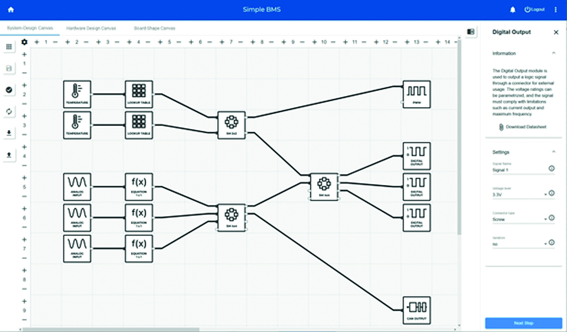
As soon as you have logged in to the Celus platform, an empty dashboard opens. The projects are created and displayed using this dashboard tool. The dashboard offers operations that can be used intuitively by the user. The process sequence essentially comprises the following four steps:
- Step 1: Describing the functionality of the electronic assembly using block diagrams, connections and parameters. A high-level design can be created on the dashboard that can be understood by anyone working on the project.
- Step 2: Select the appropriate hardware components and create the schematics using AI algorithms, but thanks to the dashboard tool, you are "always in the driver's seat" and can fine-tune the implementation by selecting components yourself (e.g. from the list of suitable microcontrollers) or replacing pins.
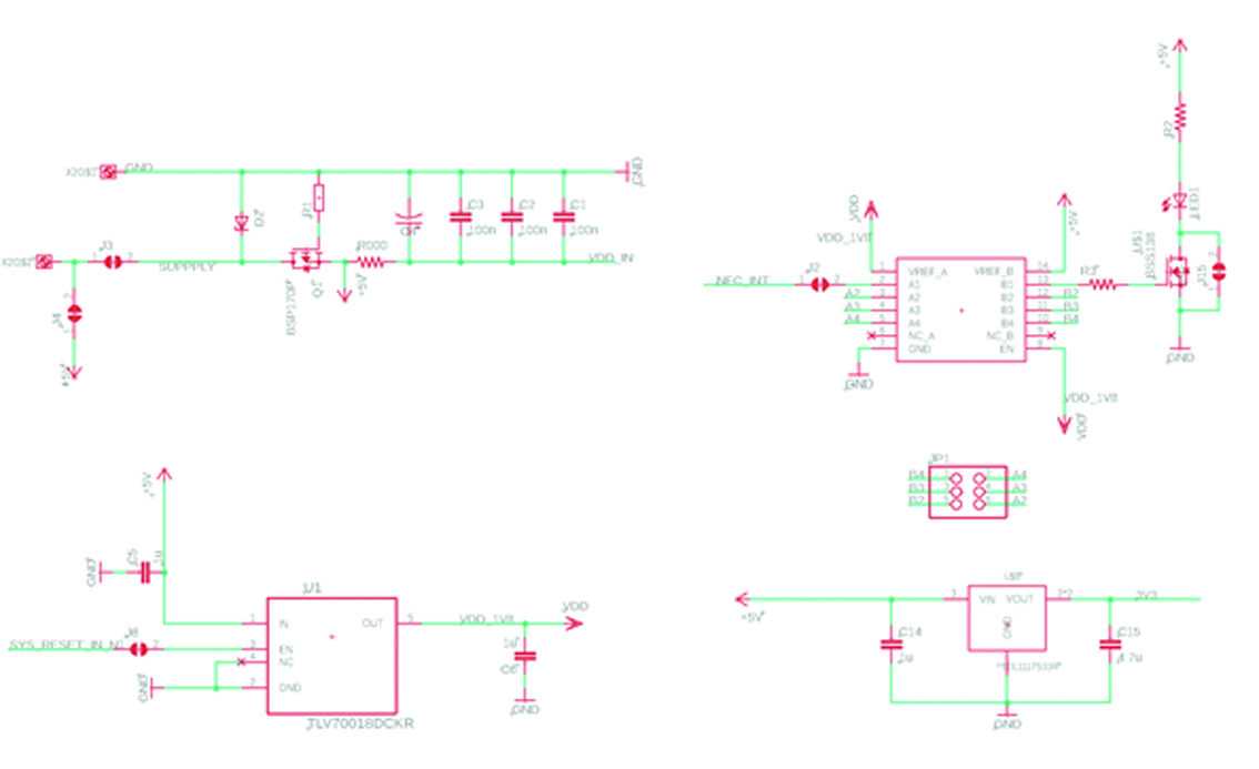
- Step 3: Describing the PCB shape and size as well as other mechanical restrictions and placing the connectors using the dashboard. The intelligent algorithms take these inputs and optimize the circuit for the application, including the creation of the schematic, layout and BOM.
- Step 4: CAD export of circuit diagram, layout and BOM to the CAD tool of your choice so that they can be further processed or modified as required (currently Autodesk Adler, Mentor PADS and Professional/Xpedition are supported, more soon).
This means you no longer have to deal with repetitive and tedious tasks such as selecting components or layout with circuit routing. The Celus software bypasses all limitations and provides a suitable solution that saves days of work. In this way, electronics engineering can be accelerated by up to 90%.
The Celus engineering platform also generates the base and application software automatically. This is done based on the selected microcontroller, the HW connections and the logic between inputs and outputs defined in the functional block diagram.
In addition, prototypes of the PCB can be requested directly from the Celus Engineering platform. An offer is then submitted online by partner companies. This ensures that high-quality hardware is supplied for the tests.
Initial application examples demonstrate the benefits
Using the Celus Engineering platform offers many advantages, including
- Complexity is handed over to algorithms so that PCB design expertise requirements can be reduced
- Collaboration across time, projects and locations is enabled
- Savings in effort, cost and time to market of up to 90%.
Initial application examples prove this and show what can be saved in reality.
Example 1: LAN card for industrial control processes
- Complexity: medium
- Number of parts: 160
- Number of connections: 2600
This highly integrated LAN card was created as a refactor of an existing design. Therefore, a predefined form factor and a specific microcontroller were important constraints to enable mechanical and code compatibility with the existing design. The PCB design was generated 100% automatically, reducing the engineering effort from 160 h to 3 h and by 90% overall.
Example 2: Wearable with environment-sensitive LEDs
- Complexity: low
- Number of parts: 100
- Number of connections: 1500
When developing the new wearable product, which is heavily dependent on user feedback, it is important to be flexible and iterate quickly on prototypes. Adding and removing sensors and LEDs to this design can be done with the click of a mouse. Again, the PCB design was generated 100% automatically and the engineering effort was reduced from 80 hours to 2 hours and by 90% overall.
The company and its milestones
When the founders took part in the TUM business plan seminar, the project and the name 'Contunity' were born. In October 2016, the company was awarded the EXIST start-up grant from the German Ministry of Economic Affairs. This grant gave the founders the means to pursue their ambitious project. Contunity GmbH was legally founded in December 2017. The founders were Tobias and Alexander Pohl. In February 2018, the software developed by Contunity was used to generate the first PCB design based solely on user requirements. In September 2018, the company received the WECONOMY Award. This gave the team access to an extensive industry network.
In October 2018, Contunity completed a six-figure pre-seed investment with electronics industry expert Dr. Dieter Lederer. With the recruitment of software engineer Rui Calsaverini in December 2018, the start-up company had ten employees. In December 2019, € 1.7 million in seed financing was provided by Speedinvest as lead investor, Plug and Play and again by Dr. Dieter Lederer.
After careful consideration, the name chosen for the product and company, Contunity, was changed to Celus in February 2020 - the legally valid renaming of the Garching-based GmbH has not yet been completed.
