Microprocessing equipment is characterized by a high surface-to-volume ratio. Due to large internal surfaces, for example, large amounts of heat can be transferred easily. The thermal conductivity of the material is no longer the determining parameter.
1 Introduction
1.1 Requirements for micro-process engineering components
Typically, micro-process engineering equipment contains structures measuring a few tenths of a millimeter. Partition walls between reaction and cooling passages are also only a few tenths of a millimeter in size. This means that large amounts of heat can be transferred in a small component volume. Even highly exothermic batch processes can be run continuously. On the other hand, the demands on corrosion resistance are increasing dramatically: it should be borne in mind that corrosion resistance is a system property that is subject to many influencing factors such as temperature, fluctuations in the media composition and oxygen content, design aspects (backflow zones, cavitation), flow velocity and side reactions. This cannot always be accurately tested in preliminary tests in the laboratory and information from material manufacturers on corrosion removal rates in millimetres per year is not useful in micro process engineering due to the small wall thicknesses and possible fluctuations under practical conditions. Therefore, very good knowledge of the occurring corrosion load and extremely corrosion-resistant materials are essential for micro-process engineering equipment. This applies, for example, to high-alloy stainless steels and nickel-based materials.
 Fig. 1: Slotted heat exchanger made of 1.4301 block, eroded: Fig. 1: Slotted heat exchanger made of 1.4301 block, eroded: left: partially eroded to measure the deformation of a 0.5 mm thick base as a function of pressure; corrugated sheets inserted to stabilize the other channels can be seen. Centre: Marking of the passage breakthrough; right: material defect (pore) in a floor
1.2 Comparison of different technologies for microstructuring
The type of microstructuring has a major influence on the overall costs of microprocessing equipment.
Iron-based materials can be chemically etched [1]. The production of a photomask is required as a fixed cost for each design. An FeCl3 etching process is used, in which problematic residual materials must be disposed of.
Passage breakthroughs due to pores or non-metallic inclusions can occur due to the small wall thicknesses of a few tenths of a millimeter in micro-process engineering components (Fig. 1).
The roughness of etched surfaces is quite high with values ofRa = 5 to 8 µm, which leads to pressure losses in microchannels.
Nickel-based materials can only be structured micromechanically. All these materials are very tough and can only be machined with great effort and tool wear [2]. While straight channels can be produced using saws, more complicated shapes can only be produced using finger cutters with a correspondingly small diameter. As the moment of resistance to bending decreases with the third power of the diameter, the mechanical stability of the tools and productivity are very low. Mechanical micro-machining becomes a cost-determining step. In addition, work hardening and distortion of thin sheets must be expected.
Laser cutting is therefore a cost-effective alternative. Productivity is largely independent of the material to be processed and the 2D structure to be produced. The material is melted in the area of the laser beam and the molten material is expelled from the cutting gap using pressurized gas. The blown-out, liquid material contains most of the energy introduced by the laser beam.
Nevertheless, there are other parameters that determine what proportion of the heat remains in the workpiece [3]: e.g. the diameter of the laser beam. It determines the maximum sheet thickness that can be cut. The thermal conductivity of the material, the cutting speed, the diameter of the cutting gas nozzle and the cutting gas pressure also play a role. The nozzle diameter in particular should be selected as small as absolutely necessary, as it has a massive impact on gas consumption and therefore costs.
If the kerf boundaries only consist of thin webs, the local temperature increase is considerable. Thermal distortion can be the result. For microprocess engineering components, however, the proportion of microstructuring in relation to the volume should be as high as possible, which requires thin webs. For this reason, filigree structures that can be produced with a fiber laser with a spot diameter of less than 20 µm cannot be realized with a 100 µm fiber optic cable, as the energy input into the workpiece is many times greater and distortion occurs.
Only continuous structures can be produced using laser cutting. The base thickness between several media passages can be easily varied using sheet metal layers of different thicknesses. There is no need to worry about defects caused by the removal of non-metallic inclusions, as is the case with chemical etching.
There is a restriction on design freedom with regard to isolated, island-shaped structures. Bars separating neighboring channels must be suspended from transverse bars at the ends.
While new masks are required for design changes in chemical etching, laser cutting can be used to react very flexibly to the modification of structures by changing the CAD program.
1.3 Joining technology: diffusion bonding
Various laser-cut sheets can then be stacked alternately with unstructured strip material and diffusion welded. The process is described in detail in [4-6]. Diffusion bonding is the only process with which it is possible to join internal cross-sections over their entire surface. The temperatures are approximately 80 % of the melting temperature. The process takes place under vacuum and with the application of an axial joining force. All layers of a component are brought into atomic contact and roughness is leveled. Atoms diffuse across the joining planes, which is also associated with grain growth. As cooling under vacuum is slow, undesirable material changes can occur depending on the furnace size and component weight. Nickel-based alloys, for example, are prone to sensitization. Various phases precipitate at the grain boundaries, which can promote intercrystalline corrosion.
The result of diffusion bonding is a monolithic component. The former joining planes are no longer recognizable. The strength corresponds to that of correspondingly heat-treated parts. Work hardening is completely lost.
2 Experiments and results
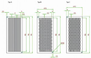
 Fig. 2: Various designs for producing different microstructures using laser cutting. Left: straight channels, middle: wavy channel structures, right: microchannels with periodic widening and narrowingWitha TruLaser Cell 3010 laser welding machine (Trumpf, Ditzingen), which was combined with a TruFiber 500 fiber laser from the same company with an 11 µm diameter fiber optic cable (LLK), cutting tests were carried out with different designs (Fig. 2). Varying 2D structures were generated over the length. Milling would be much more complex to produce, as all the material to be removed would have to be machined. For curved microstructures, sawing is also ruled out as a structuring method. With laser cutting, more complicated contours do not result in a significant reduction in cutting speed and only a slight increase in processing time due to the longer cutting path.
The structures were cut in 0.5 mm and 1 mm thick sheets of austenitic stainless steel 1.4301. The web width was identical 0.5 mm for all designs. The focal length of the collimation and optics was 150 mm in each case.
While the outer contour was produced in continuous wave mode (cw) with a power of P = 500 W, a speed of v = 20 m/min and a focus position with respect to the surface of F = 0 mm, the internal microstructures were cut in pulsed mode to reduce the thermal load on the thin webs. The peak power was P = 500 W, the average power PAV = 60 W and the pulse frequency f = 1000 Hz. The cutting speed was v = 1.8 m/min and the focus position was also F = 0 mm. A 2d cutting nozzle with a diameter of 1.4 mm and a nitrogen pressure of 15 bar was used. The distance between the nozzle and the sheet surface was 0.8 mm and was kept constant via inductive distance control. This is particularly important for very thin sheets, as these generally tend to buckle from the cutting gas pressure. At the same time, the support rails must be dimensioned in such a way that support points do not coincide with the sheet to be structured with such narrow cutting gaps, as defects occur at such points. Waste sheet strips must be held in the sheet via so-called microjoints. Otherwise they can be whirled around by the cutting gas and damage the cutting gas nozzle. The number, positioning and dimensioning of these microjoints determines the effort required to remove them.
Depending on the geometric conditions of the cut, in particular the sheet thickness, diameter of the laser beam, nozzle diameter and cutting gas pressure, heat is introduced into the workpiece. If there is little surrounding material available to absorb the heat, the temperature rise is correspondingly high and thermal distortion occurs. With pulsed laser cutting, the energy input can be controlled both in terms of distance and time. The cutting speeds decrease accordingly.
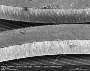
The characterization of the side wall of the webs showed that such filigree structures and sheet thicknesses of max. 1 mm can be laser-cut largely burr-free if the cutting parameters are optimized (Fig. 3).
Post-processing is not necessary. In principle, burr formation increases with the sheet thickness.
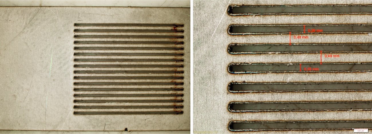
 Fig. 3: Characterization of the side walls of laser-cut webs Further tests showed that the minimum channel width that can be produced using fiber lasers can be reduced even further (Fig. 4).
It is primarily limited by the beam diameter.
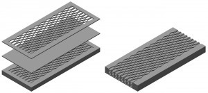
Sheets provided with microstructures by laser cutting are then stacked and joined over their entire surface by diffusion bonding (Fig. 5, left). The base thickness between passages can be easily varied to adjust the heat transfer or to achieve better corrosion resistance. The transverse auxiliary webs, which serve to fix the webs between the channels, are then removed by erosion and the channels are exposed (Fig. 5, right).
Since, as mentioned, island-shaped structures cannot be produced, process engineering effects must be realized by means of a design adapted to the production process. Conceivable options are, for example, webs inclined at +/- 45° and the staggered stacking of such sheets. This allows liquid flows to be interlaced to support mixing processes. Reaction heat can be supplied or dissipated by additional layers with transverse cooling channels.
Laser cutting with cutting speeds in the range of meters per minute allows micro-process engineering devices to be manufactured very flexibly and without tool wear.
 Fig. 4: Cutting tests to determine the lower limit of the possible web width
3 Summary and discussion
 Fig. 5: Left: Stack configuration of laser-cut sheets before diffusion bonding; right: exposing the channel structures by eroding the end faces In micro-process engineering apparatuses, considerable effort is required for microstructuring. Chemical etching is problematic due to waste containing heavy metals. Micromechanical structuring by means of sawing or micro-milling places high demands on machining expertise in the case of tough, corrosion-resistant materials such as austenitic stainless steels or nickel-based alloys. The costs are high due to high tool wear and long machining times. Work hardening, distortion of thin sheets and, in particular, burr formation must be expected. Both phenomena cause post-processing costs and are disadvantageous for subsequent stacking and joining by diffusion bonding.
Laser structuring is therefore an efficient way of manufacturing micro-process engineering equipment, even in sub-millimeter dimensions. The CAD design can be easily modified and manufactured directly without further intermediate steps or costs. This makes the technology ideal for prototypes and small series.
Non-contact machining enables the structuring of tough materials that are difficult to machine. Even refractory metals such as tantalum can be structured. For materials such as titanium and tantalum, however, inert gas must be used instead of nitrogen to prevent the formation of carbides, nitrides and oxides at the cutting edges. The processing speeds for laser cutting are usually in the range of meters per minute. With suitable beam sources, even very delicate structures can be produced without distortion.
Only continuous structures can be produced using laser cutting. Any remaining material cross-sections must be connected to the contour, which requires appropriate design. Island-like structures are not possible. Corresponding functional properties of micro-processing equipment must be achieved through production-oriented design.
In contrast to other processing methods, the wall thickness between passages can also be varied afterwards in the case of micro-process engineering devices manufactured using laser cutting. Breakthroughs between different passages due to pores or non-metallic inclusions in the semi-finished product can be reliably avoided. This is not always the case with chemical etching in conjunction with low wall thicknesses of less than 0.3 mm!
Laser structuring reduces processing times, especially for more complex 2D structures. For example, rows of very small holes that would otherwise have to be drilled mechanically can be produced efficiently. Such structures are used for the uniform distribution of media, starting from a macroscopic connection, to a larger number of parallel microchannels.
Literature
[1] Etching process, Ätztechnik Herz GmbH & Co KG, Epfendorf am Neckar, see https://www.aetztechnik-herz.de/technologie/aetzprozess/, last accessed: 04.08.2020
[2] T. Gietzelt; L. Eichhorn: Mechanical Micromachining by Drilling, Milling and Slotting, IntechOpen Ltd, London, 2012, 159-182, https://www.intechopen.com/books/micromachining-techniques-for- fabrication-of-micro-and-nano-structures/mechanical-micromachining-by-drilling-milling-and-slotting, last accessed on 04.08.2020, DOI: 10.5772/34124
[3] Variants and influencing variables of the laser cutting process, Homepage of Trumpf GmbH + Co KG, Ditzingen, https://www.trumpf.com/de_DE/anwendungen/laserschneiden/, last accessed: 04.08.2020
[4] T. Gietzelt; V. Toth: Influence of the surface condition on the diffusion bonding of micro-process engineering components, Jahrbuch Oberflächentechnik, vol. 74, Eugen G. Leuze Verlag, Bad Saulgau, 2018, 102-118
[5] T. Gietzelt; V. Toth; A. Huel; R. Dittmeyer: Determining the Dependence of Deformation during Diffusion Welding on the Aspect Ratio Using Samples Made of SS 304 (1.4301), Adv. Eng. Mater, 2017, Vol. 19, No. 2, DOI: 10.1002/adem.201600344
[6] T. Gietzelt; V. Toth; H. Lambach; R. Dittmeyer: Considerations of Microstructural Influences for Diffusion Welding of Metals in Microsystem Technology, Adv. Eng. Mater., 2013, Vol. 15, No. 8, DOI: 10.1002/adem.201200339


