As part of joint industrial research (IGF), the fem Forschungsinstitut and Hahn-Schickard have developed a new, innovative process for creating conductive structures on plastic substrates. The process combines digital inkjet printing with electroless metal deposition with the aim of producing conductive structures on different substrate materials, especially on transparent and temperature-sensitive plastic substrates.
Introduction
In conventional PCB technology, electronic circuit carriers are currently manufactured using subtractive processes. Although the lithographic and etch-based manufacturing process with copper-clad composite materials is well established, it requires long process chains up to the finished printed circuit board. In addition, subtractive processes are disadvantageous in terms of resource conservation and waste avoidance.
In the production of mechatronic integrated devices (MID), a fully additive technology based on electroless metallization is used to build up the conductor track structure. The surface of MID substrates is roughened and activated using laser direct structuring (LDS) [1]. Selective metal deposition then takes place on these areas in an electroless bath. Although a whole range of different thermoplastics are available as substrate materials for laser structuring, transparent substrates in particular cannot be metallized using this technology. Transparent substrates are, however, interesting for applications in the fields of lighting and medical technology, among others.
For many applications, full 3D capability of the structuring technology is not necessary; 2.5D structures on suitable substrate materials are often sufficient. Digital printing techniques such as inkjet or aerosol jet therefore represent an interesting alternative to previous manufacturing approaches for creating conductor track structures. The fully additive construction of the conductor track structures using metallic inks promises a short process chain and therefore, in principle, cost-effective production, particularly due to the elimination of masks and etching processes. In addition, functional printing enables the production of thin, lightweight and transparent functional components. Fields of application range from intelligent packaging to flexible circuits with so-called "system-in-foil" elements, i.e. integrated, ultra-thin components, antennas and sensors [2]. Although printed electronics in principle enable many new technical applications and offer design freedom that is difficult to realize with conventional technologies [3, 4], there are also some technical difficulties. Silver inks are usually used for the digital printing of conductor path structures. Gold, copper, platinum or alloy inks can also be used for special applications. These ink systems often have disadvantages such as a small process window during the printing process and high sintering temperatures. Furthermore, the printed structures only have low layer thicknesses and low conductivity. The inks also contain organic additives, which are usually still present in the conductor path structures after sintering. In applications in the field of medical analysis systems, these organic components can impair their function.
Combined process
In order to be able to use the advantages of digital printing without the aforementioned substrate and application restrictions for the production of conductor track structures, inkjet printing was combined with electroless metallization (see Fig. 1). This approach can be realized with the help of palladium nuclei, which act as activators. The Pd nuclei are incorporated into an inkjet printable ink formulation.
 Fig. 1: Generation of conductor structures using a combined process of inkjet printing and electroless metallization
After the printing process and subsequent drying, electroless metallization is carried out exclusively on the areas previously seeded with palladium. In this way, autocatalytic metals such as copper, nickel, palladium or gold can be deposited. In terms of substrate selection, inkjet printing is extremely versatile. Due to the comparatively low deposition temperatures in the electroless bath, the combined process also enables the use of transparent and temperature-sensitive thermoplastics such as polycarbonate (PC), cycloolefin copolymer (COC) and polyethylene terephthalate (PET) as substrates. The focus of the investigations was on PC substrates, but polyimide (PI) and epoxy resin-glass fiber composites (FR4) were also examined with regard to substrates from printed circuit board technology.
Production of the palladium nuclei
Classic colloidal Pd/Sn activators, as used in plastic metallization, are unsuitable for incorporation into an inkjet ink formulation. The Pd/Sn nuclei are dispersed in a solution with a high hydrochloric acid content, which can damage the print head. The protective colloid SnCl2, which is present in considerable excess in the activator solution, would remain in the printed structure after the printing process. In addition, inkjet ink formulations must have certain properties such as specific viscosity, surface tension and density, measured as Reynolds, Weber and Ohnesorge numbers, to ensure optimum printability. The viscosity of aqueous solutions is generally too low. Therefore, glycols, such as ethylene glycol, are often used as solvents in the ink formulations. For the dispersion of Pd activators in such an ink formulation, a functionalization of the nuclei is required. For this reason, special Pd nuclei were developed whose surface was functionalized with polyvinylpyrrolidone (PVP). PVP also serves as a stabilizer and prevents agglomeration of the particles. The functionalized Pd nuclei were produced wet-chemically using the bottom-up method [5]. The process is shown in Fig. 2a. In this process, Pd precursors are reduced in the presence of a stabilizer. The Pd atoms formed arrange themselves into clusters, which slowly grow into larger nuclei. During this process, the stabilizer attaches itself to the surface of the nuclei and thus prevents further growth. As with classic electroless metallization, only a small amount of palladium is required for the combined process. Accordingly, the Pd content in the ink formulations is also in the ppm range.
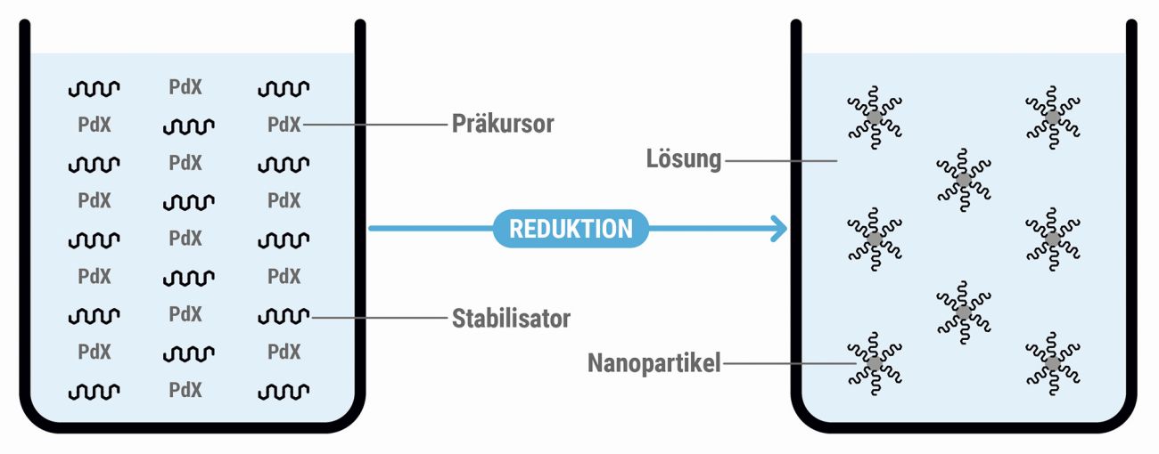 Fig. 2: a) Systematic representation of the bottom-up method
By varying Pd precursors, reducing agents and reduction conditions, Pd nuclei with a concentration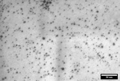 Fig. 2: b) STEM image of PVP-functionalized Pd nuclei
of up to 5000 ppm could be produced. On average, the size of the synthesized Pd nuclei was approx. 3 nm (see Fig. 2b).
Thus, the size of the synthesized Pd nuclei is roughly comparable to commercial Pd/Sn activators. Ethylene glycol and glycol ether were used as solvents for the Pd nuclei dispersions. Based on a modular principle, the Pd nuclei dispersions were then added to existing base inks. This approach to ink formulation enables simple and efficient optimization of the inks. In addition, additives can be easily added and solvents substituted. Unless otherwise stated, ink formulations with a Pd content of 500 ppm were used for the printing tests. With appropriate storage, the Pd activator solutions and the ink formulations produced from them should be stable for at least 6 months.
Ink formulations, printability and metallization
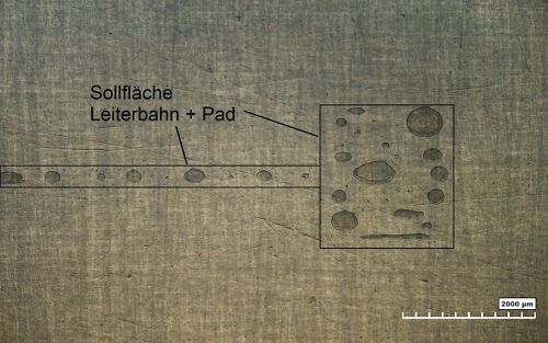
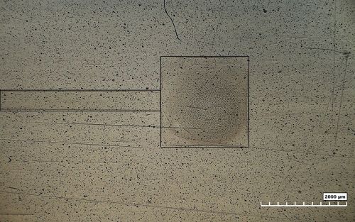
All printing tests were carried out on a Dimatix Materials Printer 2850 (Fujifilm Dimatix). An ink formulation based purely on ethylene glycol was used for the initial printing tests. To produce the ink (Pd-T-1), a Pd seed dispersion (2500 ppm) was first produced in ethylene glycol, which was then mixed with ethylene glycol at a ratio of 20:80. To print an ink using the inkjet process, a uniform drop ejection from the print head via the piezo element is required. By applying a voltage (waveform) over time, this can be varied depending on the ink properties. A waveform was successfully developed for the Pd-T-1 ink formulation. A stable printing process could be carried out over a period of several days. Printing was carried out with a drop spacing (distance between the printed droplets on the substrate) of 25 µm. When printing on PC and PI, it was found that the wetting with Pd-T-1 was too low (see Fig. 3a). To improve wetting, the substrates were subjected to atmospheric plasma treatment. By changing the surface properties (roughening and oxidation) and the associated modified wetting and drying behavior, the desired test structure could be better reproduced in the print, as Fig. 3b illustrates. Despite the improved wetting due to the pre-treatment, the Pd nuclei are unevenly distributed over the printed test structure after drying. A threshold analysis of the light and dark areas in the microscope image showed that the germs were not homogeneously distributed over the entire printed surface (see Fig. 3c/d). About 25 % of the printed area showed a high concentration of Pd nuclei, while the Pd nuclei density in the remaining areas was rather low. This observation can be attributed to the very small particle size of the germs and the associated high diffusivity. During the drying process of ethylene glycol, a concentration takes place in which locally larger agglomerates can form due to diffusion.
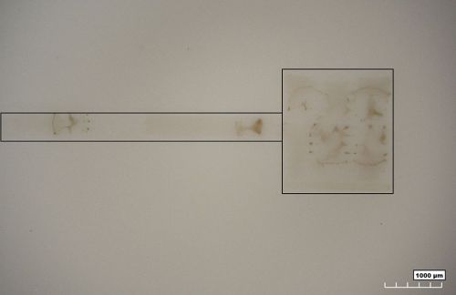
In order to improve the uneven distribution of the Pd nuclei, the print resolution was first increased. For this purpose, the drop spacing was reduced from 25 µm to 20 µm, whereby more droplets and nuclei were applied to the surface. However, this only resulted in an intensification of agglomeration and the formation of larger aggregates (see Fig. 4a/b). This observation indicates that agglomeration can be influenced by printing and drying processes. In inkjet printing, it is possible to segment the surface to be printed into a kind of "checkerboard pattern", as shown schematically in Fig. 4c . Both patterns are printed sequentially in order to obtain the desired print area. This measure reduces the maximum contiguous area to the size of a "checkerboard square". Thus, the Pd nuclei should be more finely distributed over the entire printed area. As Fig. 4d shows, the expected effect also occurs when printing Pd-T-1 in a checkerboard pattern (size 1 pixel); the palladium is distributed much more evenly over the printed area. It has also been shown that sequential printing of pads and tracks also improves the Pd distribution. This can prevent the ink from flowing from the track to the pad.
 Fig. 4: Pd-T-1 printed on pre-treated PI (total length of the printed structures: 14 mm) a) Dropspacing 25 µm
 b) Dropspacing 20 µm
 c) Division and printing sequence for "checkerboard printing" (drop-spacing 20 µm)
 d ) Printed checkerboard patternThemetallization tests were carried out with the copper electrolyte Circuposit 3550-1 (DuPont). Irrespective of the substrate used, the printed Pd-T-1 structures generally showed a poor initial behavior of the Pd nuclei in the copper bath. Very little metal was deposited on the printed areas. It can be assumed that the number of Pd nuclei was too low to initiate metallization. In order to increase the number of nuclei, several layers of ink were printed on top of each other, which resulted in metal deposition in the subsequent copper bath. However, the metallization was not adherent and the structures detached completely from the substrate in the tape test. Preliminary investigations have shown that the wetting of Pd-T-1 on the substrates investigated can be improved by adding less polar solvents with lower surface tension, such as glycol ether. The improved wetting should also increase the affinity of the Pd nuclei to the substrate surface. To create an optimized ink formulation, a Pd nucleus dispersion (2500 ppm) was prepared in glycol ether. This was then mixed with ethylene glycol at a ratio of 20:80 (Pd-T-2). The addition of glycol ether required a slight adjustment of the printing process. After several layers of printing, Pd-T-2 could also be metallized. The printed structures were reproduced somewhat better here than with Pd-T-1. However, a large part of the metal layer detached from the substrate in the tape test. Plasma pre-treatment before the printing process had no positive influence on the adhesive strength of the metal layer.
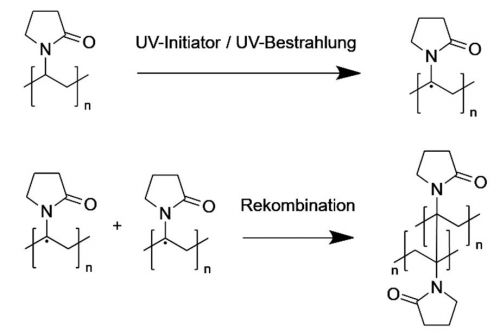 Fig. 5: Schematic representation of the UV cross-linking of PVP
Additional PVP was added to the ink formulation to increase the adhesive strength. PVP is used here as an adhesion promoter by cross-linking the PVP chains after the printing and drying process. Cross-linking is achieved with the help of UV radiation and a suitable initiator. The resulting PVP matrix bonds the Pd nuclei and the substrate together. The cross-linking process is shown schematically in Fig. 5 . The initiator generates radicals within the PVP structure under the influence of UV radiation. The recombination of two PVP radicals forms a chemical bond between the chains. The result is a cross-linked matrix.
However, the addition of PVP to the Pd-T-2 ink led to a sharp increase in viscosity, which is due to the swelling of the polymer in the ink solution. It is therefore only possible to print the ink by adjusting the solvent system. For this reason, ethylene glycol was partially replaced by a low-viscosity solvent with similar surface and evaporation properties. A corresponding ink formulation (Pd-T-3) with approx. 5 wt% PVP and a corresponding commercial UV initiator was developed. UV crosslinking was carried out in a continuous oven at wavelengths between 200 and 400 nm.
The printed and cross-linked structures were metallized in an electroless copper bath (see Fig. 6). This demonstrates that the PVP matrix has no negative influence on the activity of the embedded Pd nuclei. However, the tape test showed that the metallization was not completely adherent and partially detached.
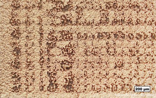
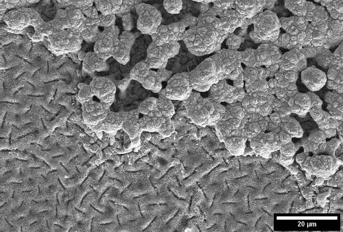
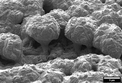
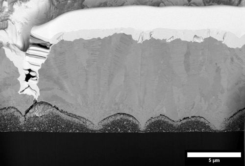
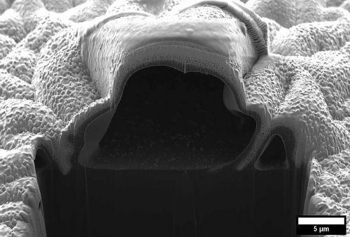
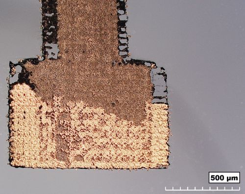 c) Overview image after the tape testIt can alreadybe seen under the light microscope (see Fig. 6b) that the copper deposition during metallization was not homogeneous. The SEM images in Fig. 7 confirm this observation. The copper layer has two different structures: "tree-like" copper structures grow up from the lower base layer to form an "upper" layer. These structures are only connected to the lower layer by a thin web and widen considerably towards the top. Only the "lower" copper layer is adhesive and survives the tape test. The FIB section clearly shows that the structures grow out of depressions in the PVP matrix. With the exception of the thin web, the structures have no direct contact with the lower copper layer and therefore only have a low adhesive strength. The cause of the indentations in the PVP matrix is unclear. To improve the metallization process, the Pd content was increased from 500 to 2000 ppm. For this purpose, a Pd seed dispersion was prepared in glycol ether with a Pd content of 5000 ppm, the dispersion was then mixed with the corresponding solvents in a ratio of 40:60 (Pd-T-4). Although the increased Pd nucleation density reduced the "tree-like" growth of the copper, it did not improve the adhesive strength. In addition, the printability deteriorated due to the increased proportion of glycol ether.
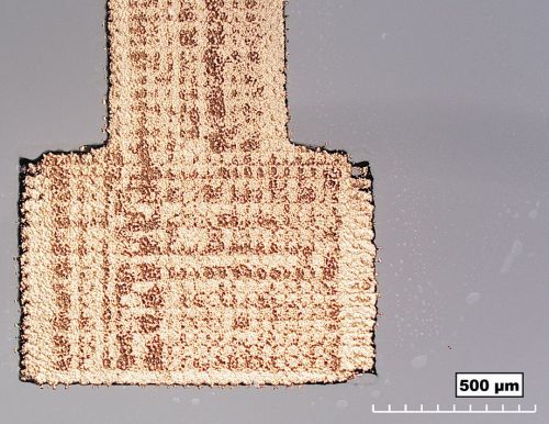
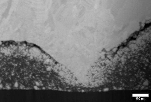
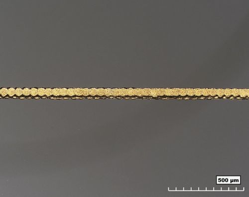
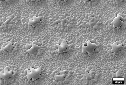
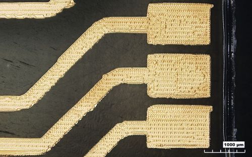
With regard to possible applications in medical technology, where metal layers containing copper and nickel are often undesirable, the printed structures of Pd-T-3 were metallized without external current with the precious metal layer system Pd/Au. The autocatalytic palladium electrolyte Altarea TPG-39 (Umicore Galvanotechnik GmbH) and the partially autocatalytic gold electrolyte Gobright TWX-40 (Umicore Galvanotechnik GmbH) were used for this purpose. The Pd/Au layer is adhesive in the tape test and has a total layer thickness of around 1 µm in the FIB section(see Fig. 8). A clear roughening of the metallized surface can already be seen in the light microscope images. The SEM images show that the metallization has elevations at regular intervals. These are larger than the "tree-like" structures in the copper deposition and do not taper towards the substrate. An FIB section through the elevations shows that these are the result of cavity formation. The cavities were probably caused by swelling of the cross-linked polymer layer in the electrolyte. Despite the swelling process, the metal layer is firmly bonded to the PVP matrix and the matrix is firmly anchored to the substrate surface. Interestingly, the swollen areas coincide with the pressure spots of the uppermost printed layer, which explains the uniform spacing of the elevations. This indicates that printing and drying processes play a decisive role in the subsequent metallization.
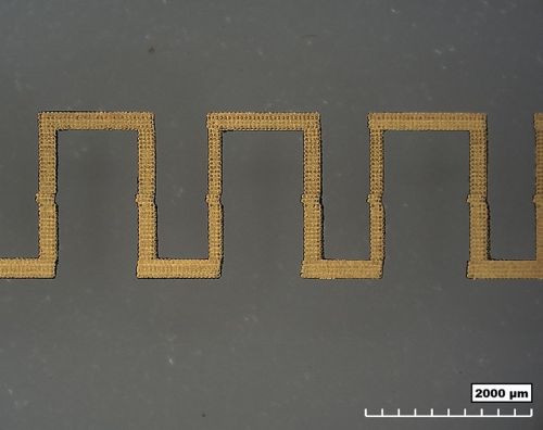
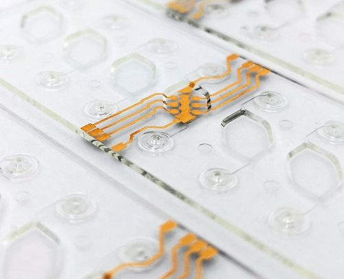
Conductor structures made of precious metals are suitable, for example, as electrodes in medical analysis systems. In order to demonstrate the manufacturability of such electrodes using the combined process developed, a technology demonstrator was constructed, the geometry and layout of which is based on an already known microfluidic chip [6]. Inkjet printing with Pd-T-3 was carried out on an injection-molded 2.5D substrate made of the thermoplastic COC (cycloolefin copolymer). After drying and cross-linking, the printed structures were metallized with Pd/Au. It was shown that both inkjet printing and adhesive metallization across radii and bevels are reproducible with the combined process (see Fig. 9).
Conclusion and outlook
The incorporation of Pd nucleus dispersions in ink formulations for inkjet printing opens up a great deal of scope in the development of ink systems. Inkjet printable ink formulations have been developed and could be printed on various plastic substrates. The Pd nuclei in the printed inks exhibited good bounce behavior in electroless metallization baths, and the printed areas were fully metallized.
The combined technology is very promising, but not yet fully developed. In particular, the need for multi-layer printing for high-quality metallization is still in the optimization phase. Electroless metallization with copper shows good results, but must be improved in the direction of a more homogeneous and uniform growth of the metal layer over the entire printed surface as well as increased adhesion strength. With regard to precious metal-based adhesive electrode structures, very good results were achieved with the electroless metallization of the printed inks with Pd/Au. The combined process of inkjet printing and electroless metallization thus demonstrates the potential for producing conductor track structures on various substrate materials for a wide range of applications.
The challenges of the combined process that still need to be solved are known. As part of follow-up projects, suitable solution strategies are to be developed in cooperation with interested companies in order to bring the technology to industrial application.
Acknowledgements
The IGF project 21424 N of the Research Association Edelmetalle + Metallchemie and Hahn-Schickard was funded by the Federal Ministry of Economics and Climate Protection via the AiF as part of the program for the promotion of joint industrial research (IGF) on the basis of a resolution of the German Bundestag.
Literature
[1]https://www.lpkf.com/de/branchen-technologien/elektronikfertigung/Laser-direkt-strukturierung-lds-von-3d-mids
[2]A. H. Dietzel, et. al, System-in-foil technology, Ultra-thin chip technology and applications, Springer, 2011.
[3]K. Hecker, Printed electronics has arrived in everyday life, CHEManager, 2019, 02
[4]E. Hopf, "3D Structural Electronics" is gaining in importance: "The key drivers are thin, flexible and light", Markt&Technik, 2018, 02.
[5]T. K. Sau, et al, Complex-shaped metal nanoparticles: bottom-up syntheses and applications, Wiley-VCH, 2012.
[6]IGF project 19364N: Universal mediator probe platform with electrochemical detection for mobile point-of-care DNA diagnostics (Mobi-E).

