Dresden/Freiberg. The hopes of subsidies from the new European chip law alone are enough to finally get microelectronics moving again in this country.
After the US semiconductor giant Intel recently decided to build several chip plants and invest billions in Magdeburg, the next big bang in East German microelectronics is now following: Infineon is building another chip plant in Dresden and investing five billion euros in it. The new mega-fab will manufacture analog and hybrid circuits as well as power electronics on a large scale on 300 millimeter (mm) silicon wafers. However, Infineon is making the major investment dependent on 'appropriate' subsidies.
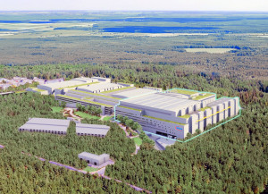 The montage shows the new planned mega fab on the far right of the picture, to the left of it the two existing 200 mm fab modules and on the far left the 300 mm fab for power semiconductors, which also already exists Infineon employs around 3100 people in Dresden and has been operating semiconductor factories in Dresden since the 1990s. These include two 200 mm modules for logic circuits, which are used in cars, chip cards and industrial machines, for example, as well as a 300 mm fab for power semiconductors. In view of rising demand, the Group had been considering a multi-billion euro expansion in Dresden for some time. The new fab will apparently primarily produce microelectronics for solar and wind power plants, consumer goods power supplies, networked electric cars and Industry 4.0. "At full capacity, the annual sales potential of the planned factory is at the level of the investment," Infineon said.
"Decarbonization and digitalization are leading to a structural increase in demand for semiconductors," said Infineon CEO Jochen Hanebeck, explaining the decision. "This dynamic has accelerated further, so now is the right time to give ourselves an even more ambitious target business model. With the planned investment in a new plant, we are continuing to implement our strategy consistently and are broadening the basis for our accelerated profitable growth course with foresight." Hanebeck anticipates strong growth momentum for Infineon from the electromobility, autonomous driving, renewable energies, data centers and the Internet of Things (IoT) segments.
"We are pleased about the political support for an investment in Dresden and are counting on appropriate funding under the European Chips Act," emphasizes Hanebeck. It can be assumed that the Infineon Executive Board will take Intel Magdeburg as an example when it comes to subsidies and consider a subsidy rate of 30 to 40 percent to be 'appropriate'. In other words, the EU, the federal government and possibly also the Free State of Saxony are expected to contribute around two billion euros.
Siltronic modernizes Freiberg wafer factory
Further up the semiconductor value chain, new impetus is also on the horizon in 'Silicon Saxony': The German silicon wafer manufacturer 'Siltronic' is borrowing 200 million euros from the 'European Investment Bank' (EIB) to modernize its Freiberg factory and to research and develop the "next generation of hyperpure silicon wafers and silicon rods". This was announced by Siltronic and the EIB.
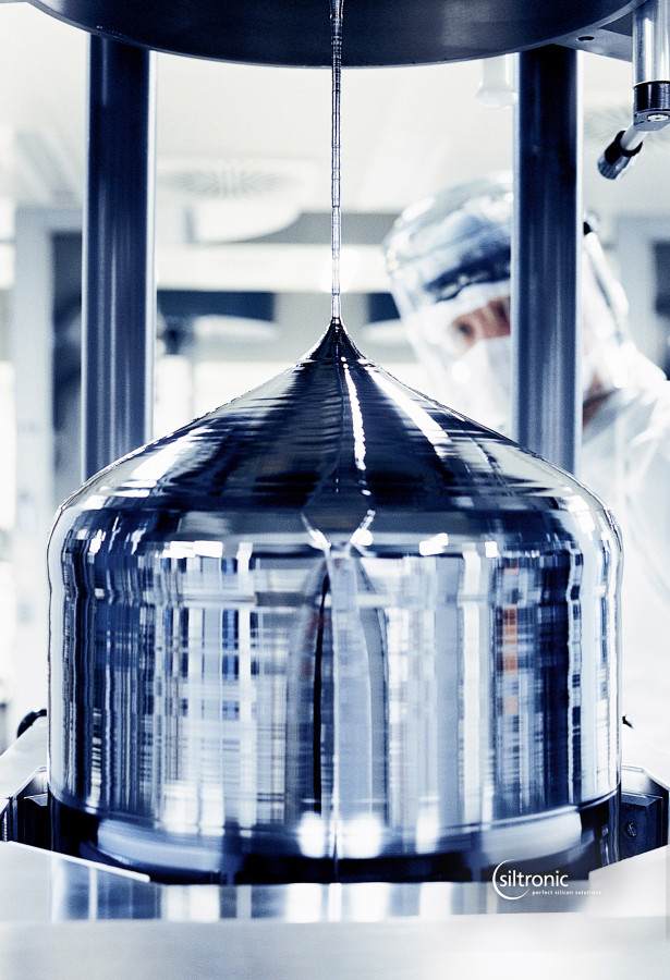 View of the crystal growing facilities at Siltronic
"With its loan, the EIB is supporting the only major silicon wafer manufacturer outside Asia, financing important investments in the European semiconductor value chain and strengthening the competitiveness of the EU semiconductor industry," the statement reads. "In our view, Siltronic is of strategic importance for Europe," emphasized EIB Vice-President Ambroise Fayolle. And because the project is being implemented in Freiberg and Burghausen, it secures jobs in Saxony and Bavaria."
Siltronic claims to be the world's fourth largest manufacturer of silicon wafers, which are primarily used in chip production. The company estimates its own global market share at 13%. The wafer manufacturer was founded in 1968 as a spin-off of the German chemical group 'Wacker'. Today, Siltronic employs 4100 people worldwide, including 880 in Freiberg, Saxony.
State-of-the-art chiplet factories soon also available for small tech companies
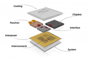 Chiplet architecture from Fraunhofer IIS/EASIn addition tothis poker game between the big players, researchers arealsoendeavoring to make top microelectronics technologies accessible to small and medium-sized companies. To this end, Fraunhofer Dresden is continuing to design a high-tech modular system that makes modern circuit technologies such as 'chiplets', which are usually reserved for large customers with mass orders, available to SMEs. The approach: in future, even small customers will be able to assemble their customized 'super circuit' (chiplet) from several individual components, which will then be manufactured in different factories using processes with different costs and finally assembled into a chip. To connect the arithmetic units, memories and other chip units, the Dresden branch of the Fraunhofer Institute 'Development of Adaptive Systems' (EAS) uses the 'Bunch of Wires' (BoW) wiring technology.
5-nanometer processes from Korea can be used
The EAS engineers have now tested the concept in practice in Samsung's foundries. This opens up the possibility for small technology companies from Germany to cast parts of their chip concepts in silicon using Samsung's advanced 5-nanometer technology.
As a reminder: Chiplets are circuits that are not produced 'from a single mold' in a semiconductor factory, but whose components are manufactured at several locations in different structure generations and processes. Finally, the client or foundry assembles the individual chips into a functional unit and contacts them - for example with 3D channels through the silicon layers. This often results in cost and efficiency gains if, for example, only a few core components in a graphics processor need to be manufactured using cutting-edge technology for performance reasons, but simpler manufacturing processes would be sufficient for other components such as memory. In addition, circuits can be realized that would otherwise not fit into a single process.
 However, the connection and logistics costs for chiplets are quite high, so that the use of this technology has so far been more worthwhile for large series. The EAS now wants to establish standardized connection technologies between individual chiplet components that make the whole concept interesting for small and medium quantities. With the wire approach, which in turn is based on the specifications of the Open Compute Project (OCP), the Fraunhofer engineers from Saxony have achieved quite high data rates: "In the project, we were even able to achieve the highest data rate of 16 gigabits per second and path required by the BoW standard," explains EAS chiplet expert Andy Heinig.
EAS was already involved in the Usep project
In the past, the EAS had already researched ways to facilitate access to the latest microelectronics, especially for the rather small-scale Saxon technology industry. This included, for example, the 'Universal Sensor Platform' (Usep) project, in which the Fraunhofer Institutes IPMS, ENAS, IZM, ASSID, IIS and Globalfoundries Dresden were involved. The partners are creating a kind of electronic modular system that can be flexibly equipped with various sensors, wireless modules and other components. Usep is primarily designed for companies that have designed their own tech products for the Internet of Things (IoT) or Industry 4.0, but do not have their own chip factory or want to build such small series that even an order for a traditional foundry would be too expensive.
'Heimdall' monitors wafer path traffic in the chip factory
 Trustworthy system integration in semiconductor productionTheUsep system is now in use in the Globalfoundries Dresden semiconductor factory, for example, for predictive maintenance of the wafer transport systems. To this end, the Dresden-based electronics company 'Deltec' has developed an artificial eavesdropping analyzer for wafer transporters together with local partners. This 'Acoustic Analyzer' should help "Globalfoundries to significantly reduce disruptions on the wafer transport route", according to Deltec.
Background: In large semiconductor plants, a kind of railroad under the cleanroom ceiling automatically transports the silicon wafers on which the circuits are created from plant to plant. However, Globalfoundries Dresden also wanted to automate the maintenance of the wagons used in this process in order to prevent unexpected breakdowns and also to avoid unnecessary and expensive periodic replacements when these so-called 'overhead vehicles' (OHV) are actually still OK.
The chip contract manufacturer asked the Dresden-based innovation agency 'Smart Systems Hub' for a solution. The agency then brought Deltec, T-Systems MMS and 'Zeiss Digital Innovation' together to form a 'digital product factory'. This swarm development network created a prototype from which the 'Heimdall' system ultimately emerged. The name comes from the fact that, like the Norse god guardian of the same name, it primarily performs surveillance work.
And this is how it works: as soon as the 'Acoustic Analyzer' hears an approaching vehicle using ultrasonic sensors, it listens to its driving noises and forwards them to an evaluation base via WLAN radio. "Atypical or inappropriate noises that indicate wear or malfunctions of the transport vehicles are filtered out," explains Deltec. "As soon as an anomaly is detected, the system alerts the employees and they can inspect the relevant transport trolley as quickly as possible and repair it if necessary. This contributes to uninterrupted production."
 Dino petting zoo in the metaverse, aka cyberspace, aka Second Life: in addition to VR data goggles, new human-machine interfaces based on "fast" technologies, such as this one for the fingers, will enable an immersive experience in virtual reality (VR)Deltecis an electronics contract manufacturer and product developer from the south of Dresden. The company was founded in 1992 from the former Robotron company 'Messelektronik', now has 60 employees and is currently expanding. The other project partners are also part of the backbone of Dresden's technology industry: Globalfoundries operates the largest chip factory in Europe in Dresden, MMS is ultimately a software forge for Telekom and 'Zeiss Digital Innovation' was born in 2019 when Zeiss took over Dresden's post-reunification start-up 'Saxonia Systems'. The Smart Systems Hub Dresden, in turn, was created as part of an initiative by Bitkom and the Ministry of Economic Affairs, which launched twelve centers of excellence across Germany in the form of 'Digital Innovation Hubs' in 2017. The Dresden hub is primarily dedicated to technology solutions for the Internet of Things (IoT), for which it forges short-term alliances between high-tech companies and individual innovators at the location. The hub also uses spontaneous swarm concepts for this purpose.
Focus on trustworthy electronics "Made in Germany"
The joint project "Distributed manufacturing for innovative and trustworthy electronics 'T4T'" follows a similar approach. In response to industrial espionage and chip supply crises, Fraunhofer Dresden is working with partners from research and industry to develop a concept for manufacturing microelectronic circuits in a highly secure manner at various locations and linking them at a trusted location. According to the Fraunhofer Institute for Photonic Microsystems (IPMS), which is leading the project, the aim is to produce "trustworthy electronics made in Germany".
In view of the particular strategic importance of this concept, the Federal Ministry of Education and Research is covering 11.75 million of the total project costs of around 16.44 million euros. In addition to IPMS, Bosch, Osram, Audi and XFAB, Nanowired, Süss, Disco and IHP, TU Dresden and the Dresden Fraunhofer Centers and institutes Assid and EAS are also involved. The results should be available in March 2025.
"The secure supply of electronic components is of growing strategic importance for Germany as an industrial location," emphasize the T4T initiators. "The increasing relocation of the production of integrated circuits to regions outside Europe increases the vulnerability to the introduction of malware and espionage functions in components supplied by contract manufacturers. At the same time, the risk of intellectual property theft of circuit designs by third parties is increasing."
On the other hand, it is unrealistic to assume that the European technology industries will be able to deglobalize to a large extent and become independent of top contract manufacturers (foundries) such as TSMC in the foreseeable future. The T4T consortium is therefore looking for ways to divide the individual process stages of the microelectronic value chains across different locations, but to concentrate "the assembly and encoding of the systems in a trustworthy environment in Germany".
Memory codes should also be unbreakable by quantum computers
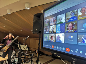 Photo: Heiko WeckbrodtTheproject partners are pursuing different approaches within this 'split manufacturing' approach: IPMS, for example, wants to integrate memorable memories with modern encryptions into the chips that cannot be cracked even by quantum computers. The Assid, on the other hand, is designing contacting techniques with which silicon wafers manufactured at different locations with chiplets and encrypted memory elements on them can be electrically or logically connected to one another. The engineers also want to solve contacting problems that can occur if the circuits on the wafers are of different sizes. And the EAS will take care of the design concepts for microelectronics from distributed production.
These efforts have complex backgrounds: Modern microelectronics value chains have long been globally distributed anyway. The core production processes ('front end') such as exposure and doping almost always take place in different factories than the contacting and final assembly ('back end'), usually even in different countries. And the installation of the circuits into complete electronic systems takes place in other factories. TSMC in Taiwan, Samsung in South Korea and Intel in the USA, for example, specialize in the core production of highly integrated chips. Many back-end factories are located in Malaysia and Singapore. Complex electronic products are assembled by Foxconn in Taiwan, for example. However, Chinese contract manufacturers are now also playing a certain role on the global market. There are also fears in Europe and the USA that China could one day invade Taiwan and take over its high-tech factories. All of this is fueling fears of dependence on and espionage by the Chinese.
In addition, the EU Commission wants to triple the global market share of European microelectronics production from seven to 20 % within a short space of time. However realistic this goal - which has already been missed once - may be, the continent will be unable to realize all links in the microelectronics value chain in Europe in the coming years: There is a lack of processor design forges, high-end factories à la TSMC, back-end factories and end-product contract manufacturers of the Foxconn class. This is another reason why Fraunhofer and other players - especially from Saxony - have been promoting the concept of virtual factories for some time, which would bring together many smaller developers and manufacturers. And a functioning 'split manufacturing' concept would be particularly important for this. Large semiconductor manufacturers such as Infineon also rely on concepts such as the virtual factory, for example in power electronics production. This should ensure that the company can quickly transfer products from one location to another and solve supply chain problems more flexibly and quickly.
'Fast' balance sheet: strong value creation matrix and technology boost for SMEs
Petting dinosaurs in the metaverse, globally networked orchestras in the real-time stream and robots for housework: within eight years, the 'Fast' cluster researchers have brought data networks and computer clouds up to speed - and are now expecting considerable economic knock-on effects. The Saxon-dominated research network has helped to shape a unique value creation matrix, spawned seven spin-offs and enabled many participating SMEs to boost their turnover and technology, according to 'Fast' spokesperson Prof. Frank Ellinger from TU Dresden.
Professors Frank Ellinger and Gerhard Fettweis had coordinated the research in the 'Zwanzig20' cluster 'Fast Actuators Sensors & Transceivers', or 'Fast' for short, since 2014. Since then, a total of 85 institutes, chairs and technology companies have significantly accelerated the wireless systems, data networks and computing clouds that we work with today and tomorrow. One aim was to drastically reduce the response times (latencies) of wired and wireless communication lines, improve their energy balance and create new applications for fast data networks. In many cases, the project partners were able to reduce these response times to just a few milliseconds, so that people hardly notice any delay when working with the cars, robots or remote-controlled factory transporters based on them. En passant, the engineers have also significantly reduced the energy consumption of these systems.
And the real-time networking of artists has proven to be a particularly popular application scenario for 'fast' technologies: English music star Jamie Cullum, for example, used the system for a remote talent search in 2019. "The number of users really exploded during the coronavirus period," reports Frank Ellinger. "We can now use it to network orchestras with up to 60 musicians."
However, the pandemic isolation has not only strengthened the need to collaborate artistically from a distance, but has also brought to the fore the question of whether only engineers and office workers can really work from home in a meaningful way, or whether factory workers can too. The Fast consortium has also come up with a solution for them, or at least an approach for teleworking in a factory: a tactile remote control for order picking trolleys in factories. They can now be controlled from home with data goggles on the nose - and thanks to short latency times of around eleven milliseconds, they also give the user tactile feedback as to whether the brake engages or the parts transporter hits something.
Other fast results could quickly pay off in the industry in euros and cents. These include, for example, a 'Power over Dataline' chip for future generations of electric cars, which Bosch was involved in developing. In future, this should ensure that data and electricity in the car flow over one line with minimal loss, which can save a lot of wiring costs. Local intelligence for car sensors and the ultra-fast synchronization of electric motors on each axle are also among the topics on which the 'Fast' partners have been working.
According to Fast spokesperson Ellinger, the fact that these and other sophisticated solutions were ultimately successful is due not least to the great depth and breadth of added value in and around the high-tech region of 'Silicon Saxony': "This meant that complete development chains from design to chip production, the development of entire systems and the programming of the appropriate software could be realized to a large extent in Saxony - although companies and institutes outside the Free State were also represented in the consortium. The result was a unique value creation matrix. "Neither China nor Silicon Valley have that," says Ellinger.
According to the coordinators, the economic knock-on effects of "Fast" are correspondingly noticeable: in the form of additional sales and new products for the small and medium-sized companies involved, but also through newly accumulated technology expertise in the region, including 16 patents. Ellinger and Fettweis are convinced that the tax money invested has already paid for itself in terms of the economic effects of Fast. In total, the "Fast" cluster had almost 60 million euros available for its research and development projects from the beginning of 2014 to the end of 2022, including almost 46 million euros in funding from the Federal Ministry of Education and Research.
The coordinators also refer to seven spin-offs that they classify as 'Fast' research: 'Siliconally' (gigabit Ethernet for cars), 'Advancing Individual Network' (optimization of wireless data networks for special applications, for example in robot-assisted factories), 'Campusgenius' (shielded private 5G networks for industrial companies, ports, etc.), 'Mimetik' (mimetic technology), 'Campusgenius' (shielded private 5G networks for industrial companies, ports, etc.).), 'Mimetik' (data gloves for the metaverse or cyberspace), 'PowerOn' (artificial muscles for robots and prostheses), 'Meshmerize' (plugging radio holes for robots and drones), Wandelbots (no-code robotics).
And although the 'Twenty20' funding is now coming to an end, this is by no means the end of the research. Prof. Ellinger compares 'Fast' to an oak tree with many shoots. Many follow-up projects are now building on the cluster that was once formed. These include the Centre of Excellence for Tactile Internet with People in the Loop (Ceti) and the projects E4C ('Extremely Energy Efficient Edge Cloud Hardware using the Example of Cloud Radio Access Network'), 'DAKORE' (data radio network with adaptive hardware and AI optimization to reduce energy consumption), '6G-Life' (new human-machine interfaces), 'Semeco' (accelerated and semi-automated certification of new medical technology using artificial intelligence), 'REC2' (Responsible Electronics in Climate Change Era - this planned project aims to reduce energy consumption in the production, operation and recycling of electronics).
New level of home robotics expected
Prof. Gerhard Fettweis predicts that the next, sixth generation (6G) of mobile communications will gradually come online from 2030. And then fast technologies will be in demand again, with home robots, exoskeletons for pensioners, tidying robots for children's rooms and other artificial everyday helpers growing into the mass market. For such close cooperation between humans and robots, the industry will even need negative latencies, adds his colleague Ellinger. This means that the machine has to 'guess' in advance what the person next to it is about to do. According to Ellinger, this can be achieved with innovative prediction models. And to meet the challenges of the future, Fettweis demands that we need to get on with the job rather than the job at hand: "We need to move away from small incremental improvements and focus more on revolutionary innovations, which Germany used to be known for."
Chip plants steel themselves against supply disruptions and energy crisis
In the meantime, however, Saxony's high-tech industry must first find answers to current challenges such as supply chain disruptions and the energy crisis. In response, the semiconductor contract manufacturer 'Globalfoundries' (GF) is relying on a multi-pronged strategy to avoid production stoppages at its Dresden chip factory. This includes multi-source approaches, larger warehouses and more material recycling. This was explained by factory boss Manfred Horstmann during the latest Globalfoundries Technology Summit in Dresden.
"Corona, the war in Ukraine, the conflicts between China and Taiwan and other factors have influenced global supply chains," Horstmann explained. This has shown that it is important for a chip company like Globalfoundries to not only keep an eye on its own suppliers, but also on the suppliers' suppliers. One example of this was the shipping accident in the Suez Canal, which caused an important part for a GF supplier to be stuck for weeks. The company has therefore developed a number of approaches to counter such problems, especially since the start of the coronavirus crisis in 2020.
For example, in the event of bottlenecks, missing material is quickly exchanged with other GF locations in the USA, Singapore or, in future, in Crolles, France. The Dresden fab has also increased the size of its warehouses. Furthermore, more materials and parts are being recycled than before. GF is also pursuing a multi-source approach, which aims to source as many process gases, doping blanks (targets), equipment parts and similar from more than one partner and more than one region of the world. A monitoring system was also set up to keep a constant eye on the current supply flows for the factory. And last but not least, GF Dresden has worked out a number of alternative transport routes for important supplies so that they do not dry up in the event of earthquakes, floods, coronavirus lockdowns or wars.
"But we are also preparing for natural gas bottlenecks," emphasized Horstmann. This is because the Dresden factory has its own gas-powered mini power plants, which are designed to ensure the electrical and thermal supply for the sensitive production clean rooms in the event of a major power outage. GF has installed redundant access points to the 110-kilovolt power grid, replaced old lights with economical LEDs in many places, has diesel-powered boilers and can also operate some systems with propane. A solar system on the factory roof is due to go into operation in 2023 and will cover around five percent of the site's electricity requirements. Horstmann also plans to cover around 20% of its current natural gas requirements with purchased hydrogen from 2025. "We have enough backup solutions to keep the factory running at all times," assured the site manager.


