This is how Wilhelm Busch saw it in a famous caricature, although an 'eaves' is not depicted here. But the basic idea is effectively conveyed because, as is so often the case, fate turns against the super-smart. Why did the EU push through a directive banning lead in most solders despite vehement protests from the electronics industry? Even though there was no evidence that it caused problems in any way - especially in the EU - as recovery was already well established? This is still a source of mystery today.
 The electronics industry was thrown from the frying pan into the fire by the ban on tin-lead soldersItwas certainly notfullythought through, as a series of problems suddenly emerged that have still not been fully resolved to this day. In addition to rising costs due to expensive and rare metal additives, higher energy consumption thanks to the higher melting point of lead-free solders and problems with the changeover, important industries such as space research are complaining about reliability problems.
There are quite a few complaints, such as the fact that lead-free solders have poorer wetting properties than tin-lead solders, which increases the risk of soldering errors. This is true to a limited extent, as it is largely temperature-dependent. The overtemperature with lead solders is far greater than with lead-free solders. But components, circuit boards and fluxes do not allow any further increase.
The increased occurrence of so-called hair crystals (now known as tin whiskers) is also criticized. These 'whiskers' are thin cylindrical filaments and prove to be brittle. It is feared - and this has just been identified as the cause of the failure in Galaxy IV satellites - that they could break off and cause electrical short circuits. Incidentally, compressive stresses increase the formation of tin whiskers.
There are a number of recommendations on what to do about these nasty rascals. But these are sticking plasters, because there is no absolute recipe for avoiding tin whiskers in lead-free solders. In principle, this phenomenon is not fully understood. The many experimental set-ups show how tin whiskers can even be grown in a planned way: by means of temperature cycles and also at constant temperature/humidity.
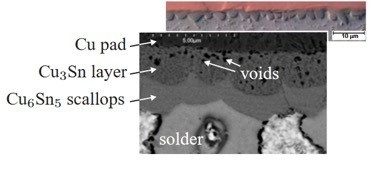
Not immediately after the soldering process, but with a time delay, more Kirkendall cavities [1] can often be detected in lead-free compounds. They are caused by diffusion of one metal into another. As the intermetallic molecules take up less space than the pure metals, space is freed up for cavities. This is not exactly favorable for long-term reliability. The higher the temperature during use or storage, the more industriously Kirkendall cavities grow, a fact that cannot be prevented in satellites, for example, during repeated exposure to sunlight and heating.
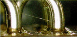 Fig. 1: The tin "whisker" shown above grows between pure tin-plated hook terminals of an electromagnetic relay similar to MIL-R-6106 (LDC 8913) Lead-containing (eutectically formulated) solder bars bend quite easily, while lead-free ones are stiffer and less pliable. A further cause for concern if vibrations or mechanical shock are feared.
For the automotive, aerospace and aviation industries, another problem is emerging in terms of ductility, as lead-free solder alloys spontaneously lose this property completely at around -30 °C - a temperature that is often reached in aviation and space.
In space, electronic products are usually exposed to a vacuum in addition to high-energy radiation. This is why there is a demand for destructive, non-destructive and accelerated tests.
However, it has been shown that the tests that have long been used (successfully?) for lead-containing compounds are not transferable on a one-to-one basis. So, to a certain extent, we are still poking around in the fog. There are still no replacements for the old test procedures.
However, these negative effects of political decisions occasionally lead to surprising findings. Researchers and engineers have been thinking about what compounds could be used instead of these tin-based solders, and one of the rather intriguing possibilities is copper [1]. It is well known that its melting point is 1357.77 K (1084.62 °C), making it unsuitable for soldering.
But the devil is a squirrel, because researchers at Lockheed Martin Corporation's Advanced Technology Center [2] have developed a nanotechnology-compatible copper-based electrical connection material that can be processed at around 200 °C. The result is a material that is suitable for soldering.
They have now gone beyond a test arrangement. In addition to a pilot plant in which nanomaterial is produced, the center has a fully functional nanocopper assembly line for process development with standard machinery.
Tests on products manufactured in this way show, among other things, that the molten material has a tensile strength that is already in the range of solders suitable for use in space.
The solder-like joining material based on nanocopper (brand name CuantumFuse) developed in this way has welcome properties [3]. In addition to the very favorable melting temperature, the compounds are expected to have up to ten times higher electrical and thermal conductivity when compared to current lead-free solders.
To better understand this actually astonishing phenomenon, one must look at the change in melting behavior as a function of size.
When the dimensions of a material become smaller and even decrease towards atomic size, the melting temperature is reduced. For metals with nanometer dimensions, this can result in a reduction of up to 100 K.
This behavior is particularly well known for nanoparticles, which all melt at lower temperatures than large quantities of the same material. The reason for the changes in melting point is seen in the much larger ratio of surface area to volume. This drastically changes the thermodynamic and thermal properties.
Requirements that are also on the table to enable use in actual soldering processes are focused on costs. This requires inexpensive syntheses for the nanoparticles with subsequent oxidation robustness and growth resistance under ambient conditions.
According to publications, good connections to Cu, Ag, Au, ENIG, Sn/SAC are achieved. The pastes melt between 195 °C to 240 °C without pressure, and solid copper is formed, which eliminates the dreaded 'whiskers', among other things. The finished compound is 'solid copper'. The melting point then increases again, which will be a challenge for any upcoming repairs.
It should perhaps also be emphasized that copper is 'cheap'. On the world market it is currently 75% cheaper than tin, costs 1/1000th of silver and 1/10,000th of gold. The buyer will have to wait and see whether the pastes currently available pass on this price advantage.
Literature:
Gary Delserro; Lead Free Solder Reliability Issues and Test Methods.
Barış Çal; Lead-Free Soldering Risks and Reliability Problems in Space Electronics; 3rd International Symposium on Multidisciplinary Studies and Innovative echnologies; October 10-11-12, 2019, Ankara, Turkey.
Alfred Zinn et al; NanoCopper Based Solder-free Electronic Assembly Material; IPC proceedings.
Lockheed Martin; CuantumFuse, A Solder Paste Based on Pure Copper; Lockheed MartinMaterials ScienceNanotechnology; October 26, 2012.
K. SCHNABL et al; Nanocopper Based Solder-Free Electronic Assembly; Journal of Electronic Materials; Vol. 43, No. 12, 2014.
https://static1.squarespace.com/static/5d2e508a028fb500010380ec/t/5d44bdd34cbc950001183210/1564786134008/Kuprion+CuantumFuse+Nanocopper+dispensable+and+stencil+printable+solder+pasteTDS+Rev01.pdf (Abruf: 21.12,2023).
https://nepp.nasa.gov/whisker/background/index.htm (Retrieved: 21.12,2023).
Wolfgang H. Müller et al; On the effect of Kirkendall voids on solder joint reliability; PAMM - Proc. Appl. Math. Mech. 7, (2007)
References:
[1] https://en.wikipedia.org/wiki/Kirkendall_effect (Retrieved: 21.12,2023).
[2] https://de.wikipedia.org/wiki/Kupfer (Retrieved: 21.12,2023).
[3] https://www.lockheedmartin.com/en-us/capabilities/space/atc.html (Retrieved: 21.12,2023).
[4] Inventor: Dr. Alfred Zinn

About the person
Prof. Rahn is a globally active consultant in connection technology. His book on 'Special Reflow Processes' was published by Leuze Verlag. He can be contacted at

