Oh, if only the world were as ideal as we secretly wish it were. Then perhaps even in the production of electronic goods the circuit board would be designed in such a way that it could actually be assembled and soldered without having to perform headstands. But where can you find a layout artist who has not only learned her profession, but also moves with the times? Fast-moving as the electronic trade is, you can't rest on your four (or is it more?) letters.
However, the gap between layout and production and then on to management is often so deep that the ideal image of one or the other cannot or must not be scratched by complaints or even suggestions for improvement. The man at the bottom of the totem pole is probably the one in production.
However, as the effects manifest themselves in a high number of errors or - even more critically - in a disappointing initial yield, the troubled process engineer must now consider what can be done about it now that everything has been concreted over and changes to the layout are no longer feasible.
Obviously, he cannot eliminate all errors with a magic wand, so that tricky and expensive rework, which also has a negative impact on the quality of the product, simply disappears. Nevertheless, he should analyze which errors occur, which are particularly critical, and whether there are ways to gradually reduce at least some of them.
 Fig. 2: Nice solder balls on the component and just look at the pad design (!)The modus operandi depends on the knowledge and skills of the process engineer. On the one hand, he can focus on the soldering defects that are easiest to rectify, on the other hand, it would perhaps be advisable to focus on those that occur most frequently, because if you can eliminate these, you have the greatest gain. The faults that cause the most impressive and therefore most expensive repair work may also be a target for remedial measures.
As the hot soldering iron is already being diligently fiddled with on the assembly, it can be assumed that someone has defined the 'faults' with sufficient precision in advance, which unfortunately is rarely the case. The engineer can therefore consider how she can reduce or even eliminate certain defects that occur during production by taking additional measures, despite the poor specifications in the layout. To do this, she has to rummage through her wealth of experience or search the relevant literature to find additional factors that she can change during production.
Two areas immediately come to mind here: assembly and paste printing. Let's leave the BGA issue aside for a moment and use the example of the 'mid-chip solder ball' for a change, i.e. a solder ball that settles between the landing areas of a 'chip component' - typically caused by an unintelligent layout error because the landing areas were designed too large and incorrectly positioned and not adapted to the chip to be used.
It seems human nature to then cap the well once the child has fallen in. The coffin lid may then serve as a model. Accordingly, an attempt can be made to correct this soldering error with some kind of fiddling. To do this, you analyze how it arises and discover that paste from the pads flowed under the component during the reflow and then unfortunately did not return to the solder joints as it should have, but instead formed this tricky solder bead.
A number of factors come to mind for the development of the error - such as the component placement, which perhaps exerts too much pressure on the paste deposit and crushes it?
So the lady checks whether the pressure or distance to the LP surface is set correctly. Perhaps the belt with the components is not clamped correctly or the components are of different dimensions. The vacuum nozzle may also be dirty.
 Fig. 3: Formation of the solder bead during the melting of the pasteThepaste itself can of course be at fault, as you will notice during tests that different pastes have different tendencies to run out. If you are allowed to play with the paste, choosing a 'better' paste can have a favorable effect - although this may then give rise to other problems.
Perhaps you can tweak the reflow profile, which could also be responsible as an ingredient, as other researchers have found out.
The paste pressure and thus the stencil are certainly not overlooked, and resourceful minds have quickly discovered that if you reduce the amount of paste on the poorly designed pads, there is less paste available when running. Whether this 'starvation' means that the resulting solder joint will last as long as desired under load is best left to the customer.
With such measures, it is important not to simply proceed in the same way for all components without discrimination. Whoever is responsible should take the time to analyze for which components a reduction in the application quantity - and by how much - is helpful. There are now suggestions in the literature that the effects should be considered before reflow under X-ray systems, because even minor changes to the shape of the recess in the stencil can achieve the desired effect, depending on what the metallization and coating on the component actually looks like.
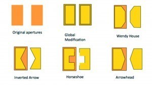
 Fig. 4: Some of the desperate suggestions to reduce the amount of pasteAdiscussion with the purchasing department canalsohelp if the process engineer has found a more suitable component (with the same properties and measured values). Perhaps he can argue that not only the cheapest component is decisive for the total costs, but that the costs for any faults that occur and their rectification should also be taken into account?
Literature and comments:
K. Bryant; M. Popovics: An Interesting Approach to Yield Improvement, SMTA Proceedings
C.Benedek: Detection of soldering defects in Printed Circuit Boards with Hierarchical Marked Point Processes, Pattern Recognition Letters 32(13), October 2011
S. Öztürk; B. Akdemir: Detection of PCB Soldering Defects using Template Based Image Processing Method, International Journal of Intelligent Systems and Applications in Engineering; 28/12/2017
H. Yamazaki: Solder Joint Integrity Test for Finding Latent Defects in PCBs, Circuit Assembly, November 30, 2001
G. Smith: Improve SMT Assembly Yields Using Root Cause Analysis in Stencil Design, IPC Apex Expo Technical Conference Proceeding, 2017
K. Pigeon: Advanced Issues in Assembly: Part 2 Causes and Cures in Solder Beading, Surface Mount Technology, November, 2001
Katherine Wilkerson et al: Understanding the Effect of Process Changes and Flux Chemistry on Mid-Chip Solder Balling, IPC APEX EXPO Conference Proceedings
References:
[1] Baruch de Spinoza (1632-1677), actually Benedictus d'Espinoza, Dutch philosopher, source: Spinoza, Ethics, presented according to the geometrical method (Ethica Ordine Geometrico Demonstrata), written in 1665, published posthumously in 1677
 Prof. Rahn is a worldwide consultant in connection technology.
 His new book on 'Special Reflow Processes' was recently published by Leuze Verlag. He can be contacted at


