While virologists, epidemiologists and, above all, politicians, who have had no training in this area, are poking around in the fog trying to contain the Covid-19 pandemic, we know far more about soldering.
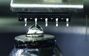 Solderability test Instead of a disease with potentially tragic consequences, soldering involves errors that can also lead to a heart attack in the end product. The solderability of components is directly related to the actual soldering defects, i.e. those that are due to wetting and not to other defects such as printing errors. If the connection of the component cannot be soldered or can only be soldered poorly, or if the contact surface and through-hole plating of the circuit board are defective, then the solder joint cannot be created, or at least not optimally.
In contrast to the origin of the virus, the cause of poor solderability of component connections and PCBs is well known. On the one hand, there are poorly controlled manufacturing processes, and on the other, contamination from packaging, shipping or handling.
Particularly during prolonged storage, metallic coatings can lead to the growth of the intermetallic zone, which can lead to dewetting once a certain thickness has been reached. In the case of organic and non-metallic protective coatings, polymerization processes are more likely to occur, which can then hardly be attacked by the flux.
If the manufacturing processes are left to the producers, there is still a wide area for the solderer to control. Starting with the purchaser and the more or less trustworthy intermediary, he has to decide where to check. Incoming inspection and additional quality control before the components and PCBs are used are the order of the day.
A statistically relevant selection alone poses a problem, because testing only the first component on the line or the top PCB in the stack is not the right method. It is worth testing on arrival, as the product will not improve if it is stored for a long time. You should also be aware that you very rarely receive completely fresh goods. If the goods are then delivered to production, a lot can still happen. It has happened that components and circuit boards with oily machine parts were left in the warehouse or rolled into boxes in which such parts had left a layer of black mass several millimeters thick. The hands of the colleagues in the warehouse didn't exactly look freshly washed either.
 The hands of the colleagues in the warehouse didn't exactly look freshly washed either (Image: CC0 1.0 Universal (CC0 1.0))Solderability tests require a certain amount of knowledge. Not only must the tester be familiar with some of the standards (MIL-STD-883 method 2003, EIA/IPC/JEDEC J-STD-002, IPC J-STD-003C-WAM1&2 with addenda 1 & 2) - he should also be aware of their shortcomings.
With both the dip-and-look method and the wetting balance solderability test system, it is not only essential parameters that need to be checked. There are also potential problems with interpretation.
The fluxes, solder alloys and temperatures are specified in the standards, probably with the clear idea in mind: if it works with these, it will solder well otherwise too. You have to decide for yourself whether this is relevant for your own production. It may be that expensive components that deliver perfectly acceptable results with the fluxes or soldering temperatures used in-house are eliminated.
However, if you change these specifications, the dear (possibly military?) customer may complain that the target devices of his ball syringes were not manufactured according to the specifications.
The standards also describe what is acceptable - about 95% coverage of the component wire after dip soldering, so pinholes, bald spots, porosity, non-wetting or dewetting must not exceed 5% of the total dipped area, although most inspectors will probably have difficulty distinguishing non-wetting from dewetting. Especially if the defects are very small in area.
 Graphic 1: Graphic representation of the procedure with the wetting scale
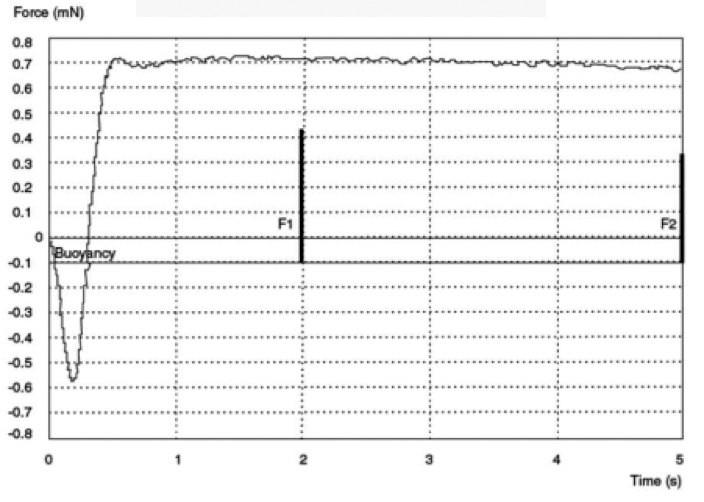 Figure 2: The 'ideal' result of the test is such beautiful wetting curves
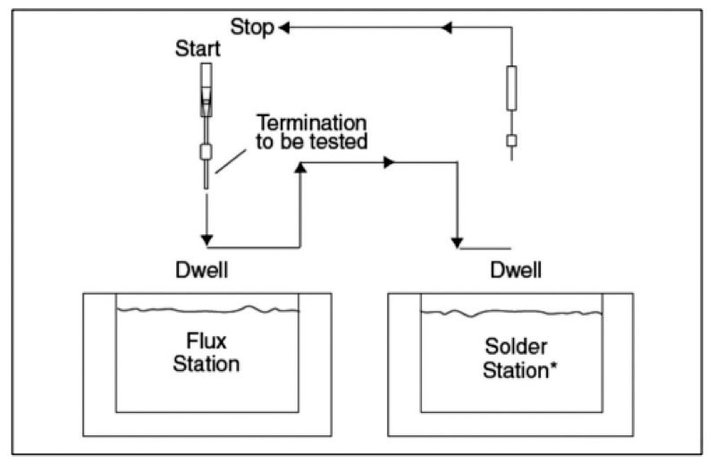 Figure 3: Principle of the dipping process
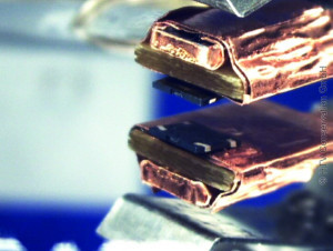
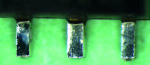 Fig. 1: Different wetting quality for three connections of a componentThestandards do not, however, describe 'where' these 5 % defects may be. This is a real shortcoming, as you will soon realize after some consideration. You may also be wondering how your quality control department or laboratory determines or calculates these '5 %' exactly, as they are not necessarily contiguous. It is generally looked at with a magnifying glass of 10 X magnification. Why 10 X in particular?
For all these processes there are now nice machines that automatically apply the 'correct' flux and also immerse the connections in a 'static' solder bath at a uniform temperature of 245 °C ± 5 °C. Apparently the temperature of the flux bath is irrelevant, as is the immersion depth in the solder bath ... and why is it a static bath when using a wave soldering process? Is the transport time between the flux application and the solder bath the same as in your machine, and why is there no preheating to vaporize at least some of the volatile parts of the flux?
With the wetting balance, several experts have found that the curve changes when wires (on the same component!) have changed in thickness or when the immersion depth is not strictly adhered to.
 Wetting testThediagram starts with a negative wetting force (first rejection of the solder during immersion before wetting begins - buoyancy force!), which increases until it crosses the zero axis of the wetting force (actually the weight of the solder on the wire), indicating that wetting has taken place. The time required for wetting is a parameter used to assess solderability. However, probably due to the difficulties of interpretation mentioned above, there are no established industry standard 'pass/fail' criteria for wetting balance analysis, which is why it is mainly used as a development tool rather than for production monitoring. The wetting force also depends on the density, composition, temperature and surface tension of the solder. Possible oxidation of the bath surface can also have an effect, but this can be largely suppressed by an inert atmosphere (nitrogen).
This may leave the printed circuit board for later.
Literature
ECIA/JEDEC Experimentation on Solderability Test Preconditioning, Volume 2, Number 1, December 16, 2019.
EIA/IPC/JEDEC J-STD-002D; Solderability Tests for Component Leads, Terminations, Lugs, Terminals and Wires
IPC J-STD-003C-WAM1&2 with Amendments 1 & 2; Solderability Tests for Printed Boards
MIL-STD-883 Method 2003
JESD22-B102; and 5) Part 21 of the IEC 60749
Image sources
Fig.1: www.doeeet.com/content/testing-eee-parts/physical-mechanical-assembly/mil-std-883-method-2003-solderability-testing/
Graphics 1-3: Reid Henry, The Role of Solderability Testing and Its Importance in Successful Soldering: www.rpsautomation.com/wp-content/uploads/2022/03/The-Role-of-Solderability-Testing-and-Its-Importance-in-Successful-Soldering.pdf


