Meanwhile, engineers in Saxony want to close a strategic processor design gap in Europe
In view of the almost constantly increasing demand for semiconductors worldwide - even before coronavirus - Jenoptik is now making the largest investment in its post-reunification company history: the chip plant supplier is building a new factory for lithography micro-optics in Dresden. Meanwhile, engineers in Saxony have set themselves ambitious challenges. They want to close a key electronics design gap in Europe, bring the first hybrid quantum communication networks to practical maturity and make circuits energy self-sufficient.
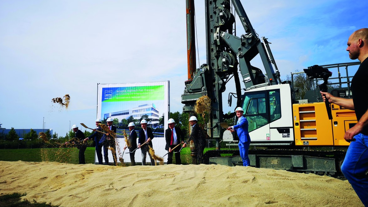
 This is what the new Jenoptik factory for micro-optics in Dresden will look like. Visualization: studiobrand.3dvisuals for JenoptikInresponse to years of rising demand for chip factory equipment, Jenoptik is now building a new micro-optics factory in Dresden. The plant, located next to the Bosch chip factory, will produce special micro- and nano-optics for the microelectronics industry from the beginning of 2025. Jenoptik intends to double its workforce in Dresden to around 120 employees. The company is expected to invest over €70 million in the factory - without subsidies. This is the largest single investment in the Thuringian company's three-decade post-reunification history.
"Dresden will become a main location for our micro-optics activities," promised Jenoptik Executive Board member Stefan Traeger. "We have deliberately chosen one of the most important locations for the semiconductor industry in Germany and Europe, where many global companies and research institutions in the sector are present."
Anchored vibration-free with 200 piles on Lusatian granite slab
 Corenext project manager Michael Roitzsch and co-managing director Tim Hentschel are working at the Barkhausen Institute on trusted processors, operating systems and open network architectures for 6G and the European telecommunications industry, among other thingsThefactory itself will comprise around 11,000 square meters of floor space, including 2,000 square meters of clean room. It will be anchored vibration-free with 200 bored piles on an underground slab of Lusatian granite: the sensors and optics that Jenoptik wants to manufacture here are as sensitive as computer chips during production. A small vibration or a tiny speck of dust can turn the entire day's production into rejects. This is because optics, which are used to align and expose chip masks over the silicon wafers with high precision, should not be thought of as lenses for spectacles. Rather, they are structures, some of which are only nanometers in size, with which invisible light beams can be directed and manipulated. Chip factories need such optics both for classic lithography with "deep ultraviolet light" (DUV) and for semiconductor structures that are produced with extreme ultraviolet rays (EUV), such as those used by TSMC in Taiwan.
In addition to chip production, such micro-optics are used in other technological manufacturing processes. These are mostly processes in which high-precision and/or very flexible positioning of light is required, for example in laser material processing or quality assurance in inspection processes. The very light and small individual components, often only a few micrometers in size, can be combined to form miniaturized scanning and switching systems with a wide range of flexible applications.
Jenoptik has been present in Dresden since 2007. Around 60 specialists are already producing such micro-optics in a building on the former ZMD campus. Jenoptik is now focusing on a larger solution and is building its own factory in the so-called "Airportpark".
At the same time, the investment once again demonstrates the long lead times required to respond to chip bottlenecks such as those recently experienced during the coronavirus crisis: First, key suppliers such as lithography equipment manufacturer ASML from the Netherlands or micro-optics supplier Jenoptik have to ramp up their own production. And then, in the best-case scenario, it will take another two to three years until a new semiconductor factory is built and equipped and the production of a new circuit functions stably and with high yields.
") Researchers, politicians and engineers in industry have high hopes for quantum technologies such as quantum communication and quantum computers (Visualization: Chair of Technical Design at TU Dresden)
Researchers, politicians and engineers in industry have high hopes for quantum technologies such as quantum communication and quantum computers (Visualization: Chair of Technical Design at TU Dresden)
The complex processes during wafer processing cannot always be fully monitored in real time - and the run-in curve for new chips also depends on this. A team of researchers at TU Dresden has therefore developed "Advisory Data Modeling" (ADM) analysis software that models such processes in the semiconductor industry, but also in other technology sectors, using data that has already been obtained. ADM then uses this data to determine how heat, humidity, pressure or other influencing factors have affected the quality of the finished product, even if this cannot be measured directly in the machine. And finally, this digital expert then gives the user suggestions for improvement.
"My goal was to create a program that was so simple and intuitive that even my mother could use it," says Hellmuth Kubin, who started developing this software in Dresden almost four decades ago and is now 77 years old himself. "Unlike conventional solutions, our software does not require the user to have any math or programming skills." The predecessor of today's software already proved its worth in GDR microelectronics.
 An employee refines GaAs wafers into power semiconductors in a high vacuum on this 35PE system at the Dresden Technology CenterMeanwhile,other research teams at the University of Dresden have turned their attention to challenges that point far into the future. For example, the privately organized Barkhausen Institute Dresden, which is docked to the TU, has now launched the €13 million EU-funded "Corenext" project, which aims to close an important gap in the value chains of European microelectronics. The focus is on the ability of Europeans - especially after Brexit and the sale of the chip architecture company ARM - to design their own fully-fledged next-generation processor cores.
To this end, Dresden-based mobile communications guru Prof. Gerhard Fettweis has forged a consortium of 23 partners, including Nokia, Ericsson, Infineon and NXP. Within three years, the participating companies and research institutes want to design their own processors, antennas, reliable architectures and operating systems for the mobile communications of the future.
"At the end of the project, we want to present the prototype of a multiprocessor system, which European telecommunications and semiconductor companies can then use to build their own circuits," announced Institute Managing Director Tim Hentschel. On the way to 6th generation mobile communications and later telecommunications standards, 'Corenext' should secure important competitive advantages for the local industry and make Europe less dependent on key supplies from the USA and Asia.
The researchers are also working on decentralized and open-source network architectures (Open RAN) that are no longer tied to the special devices of a few manufacturers, but instead handle many tasks using standard technology in cloud data centers. This should create better opportunities for smaller technology companies in particular to get involved in the large market for professional telecommunications technology with adapted standard hardware.
. Diese ermöglichen den autarken Betrieb von Mikrosensorik für den Einsatz unter anderem im Blut") A biocompatible energy storage system consisting of 90 flexible and implantable nano-biosupercapacitors (nBFCs). These enable the self-sufficient operation of microsensor technology for use in blood, among other thingsTheproject is of particular strategic importance for the EU and the new "European Chip Law", which Commission President Ursula von der Leyen (CDU) recently presented: After all, inventory analyses had repeatedly shown that the European Union not only lags well behind Taiwan, South Korea and the United States in the production of highly integrated circuits in the structural class below ten nanometers (millionths of a millimeter) and in terms of chip factory capacities, but also in circuit design. The researchers and engineers at "Corenext" therefore also want to reduce glaring technology gaps in processor design in Europe by the end of 2025.
A biocompatible energy storage system consisting of 90 flexible and implantable nano-biosupercapacitors (nBFCs). These enable the self-sufficient operation of microsensor technology for use in blood, among other thingsTheproject is of particular strategic importance for the EU and the new "European Chip Law", which Commission President Ursula von der Leyen (CDU) recently presented: After all, inventory analyses had repeatedly shown that the European Union not only lags well behind Taiwan, South Korea and the United States in the production of highly integrated circuits in the structural class below ten nanometers (millionths of a millimeter) and in terms of chip factory capacities, but also in circuit design. The researchers and engineers at "Corenext" therefore also want to reduce glaring technology gaps in processor design in Europe by the end of 2025.
Other microelectronics engineers in Dresden are now focusing more on practically applicable quantum communication technology: the engineering teams at TU Dresden are coordinating the "Quiet" and "QD-CamNetz" projects, which aim to make quantum technologies economically viable for communication purposes as quickly as possible. The federal government is very interested in these projects and is funding them with €13 million.
Specifically, TU Dresden, the University of Munich and the Leibniz Institute for Solid State and Materials Research (IFW) Dresden want to design hybrid communication networks in the joint project "Quantum Internet of Things" (Quiet) that are capable of recording the huge amounts of data in the growing Internet of Things (IoT). To this end, the partners first want to construct quantum memories and quantum sensors, which they will then network with conventional computers at the edge of the network ("edge computing") via quantum connections. They want to implement sensors with semiconductor quantum dots.
World's first 5G quantum campus network planned
The "Quantum Wireless Campus Network" (QD-CamNetz) project, on the other hand, aims to create the "world's first 5G quantum campus network", according to TU Dresden. This refers to compact systems that can be used to quickly and flexibly set up wireless and wired networks in factories, laboratories or fields that work with quantum technologies as well as with 5G and similar classically based wireless methods.
To this end, TU Dresden, the Technical University of Munich, IFW Dresden, the Dresden university spin-off Campusgenius and Deutsche Telekom want to construct special distributors ("quantum routers") that can coordinate light particles ("photons") with quantum data in the network. They are also planning to design a special quantum protocol stack. This is a kind of virtual "manual" for network control. The special highlight here is that these new instructions should enable the campus network to execute both quantum commands and conventional tasks. The highlight of the project will be a demonstrator that can set up such localized quantum networks on the TU Dresden campus. Project partner Campusgenius had previously developed mobile campus network systems for the 5th generation of mobile communications (5G).
"Campus networks are of great economic importance for industry and for the technological sovereignty of Germany and the EU," emphasize the initiators from TU Dresden. "On the one hand, this will create a globally unique hub for teaching and training quantum engineers in Germany." Secondly, Germany could set standards for the future industrial use of quantum technologies.
 Hiperscan boss Alexander Wolter shows one of his Apoident devices, which can check what is contained in pharmaceutical samples using non-contact NIR spectroscopy Another trending topic in Saxony's semiconductor industry is and remains power electronics. On the one hand - as with the expansion programs at the Infineon factories in Dresden - the focus is on higher quantities. On the other hand, however, innovators beyond the established corporate structures are also concentrating on new high-voltage semiconductors. For example, the comparatively young and small company "3-5 Power Electronics" from Dresden has, according to its own information, now brought diodes made of gallium-arsenic compounds for voltages of around 1200 volts to series production.
According to 3-5 PE, the high-voltage diodes made from gallium arsenide (GaAs) switch more efficiently than corresponding power converters made from conventional silicon, but are not as expensive as diodes made from silicon carbide (SiC). The Dresden engineers see useful applications for their mid-range diodes wherever high currents and high voltages need to be directed or controlled. This could be, for example, power electronics that convert direct current from solar systems into alternating current, but also components for fast charging stations, wireless charging stations for electric cars, plasma welding devices and other industrial electronics.
Volker Dudek, Gerhard Bolenz and Richard J. Kulle founded "3-5 Power Electronics" at the beginning of 2016. Their focus: to make gallium arsenide semiconductors, which have long been used for low voltages, usable for high-voltage applications. "The most important reason for locating our company in Dresden is the very concentrated research and service landscape in the field of semiconductor technology," emphasized "3-5 PE" development managing director Volker Dudek. The company cooperates with the Bergakademie Freiberg, the TU Chemnitz and the Helmholtz-Zentrum Dresden-Rossendorf (HZDR), among others. The team now comprises ten employees. Part of the production is carried out by "3-5 PE" in its own clean room in Dresden, while the contract manufacturer "Azur Space" from Heilbronn takes over further production steps. The Dresden-based company initially wants to sell its diodes primarily in China and Japan.
Self-sufficient chips: up to 300 milliwatts per cubic centimeter achieved
The energy consumption of electronic components and sensors is also the focus of a development driven forward by the Fraunhofer Photonics Institute IPMS and Globalfoundries in Dresden: They have managed to successfully integrate pyroelectric energy harvesters into circuits. Energy harvesting is intended to enable such chips to supply themselves with power in future.
According to Fraunhofer and Globalfoundries, these energy harvesters now achieve yields of up to 300 milliwatts per cubic centimeter. This may not sound like much, but combined with energy-saving microelectronics, it could be enough to power many sensors that are used in fields or orchards far away from any power supply for years to come. The engineers have embedded this technology in the "FD-SOI" transistor architecture from Globalfoundries Dresden, which is already designed for low energy consumption. This development was made possible by grants from the microelectronics program for "Important Projects of Common European Interest" (Ipcei). The subsidies for the Bosch chip factory in Dresden, for example, also came from these funding pots.
Prof. Oliver G. Schmidt has also been working on energy harvesting for years. However, the head of the new Center for Materials, Architectures and Integration of Nanomembranes (MAIN), who works in Chemnitz and Dresden, is looking less for self-sufficient energy sources for chips and more for his micro- and nanorobots, which he produces using nano-origami folding technologies. Among other things, he is focusing on microscopically small batteries for "smart dust". This electronic dust consists of tiny grains with a certain degree of intelligence of their own, which are supposed to combine to form swarms. Such dust storms could then be dropped in disaster areas with collapsed infrastructures, for example, to set up ad hoc radio networks or search for missing persons using a large number of sensors. One idea is that the smart dust particles could meet their energy requirements from the omnipresent electrosmog or from the Earth's magnetic field.
However, tiny medical laboratories, which are to be inserted into the bloodstream of cancer patients, for example, in order to find residual metastases and combat them radiologically or pharmaceutically, will also need their own energy harvesters. Schmidt and his team have constructed tiny biosupercapacitors for this purpose - around 3000 times smaller than all previous energy storage devices of this kind.
"The architecture of our nano-bio-supercapacitors offers the first potential solution to one of the biggest challenges - tiny integrated energy storage devices that enable the autonomous operation of multifunctional microsystems," emphasized Dr. Vineeth Kumar from the Schmidt team. The researchers are convinced that this brings the use of tiny medical robots ever closer: "It is extremely encouraging to see how new, extremely flexible and adaptive microelectronics are making inroads into the miniaturized world of biological systems," explained Professor Schmidt. This technology could lead to innovative therapies against carcinomas and pandemic viruses in the near future, but could also enable new testing technology much sooner, whether in medicine, the food industry or pharmaceuticals.
Hidden champion: Mobile Hiperscan spectrometers analyze material samples without contact
Finally, we would like to mention a "hidden champion" from Saxony that has risen to become the market leader in a niche market, but has hardly become known to the wider public. We are talking about the Dresden-based Fraunhofer spin-off "Hiperscan", which also specializes in innovative analysis devices, but on a completely different technological basis: since it was founded in 2006, the Dresden-based technology company has already supplied over 5,000 pharmacies with special infrared spectrometers that detect what is contained in a substance sample without contact. This is particularly important for pharmacists in order to check the authenticity and correct chemical composition of raw materials, from which they then mix skin ointments, individual cancer drugs or other medicines. But pasta factories, meat processors and other food companies also use Hiperscan technology to determine the fats, proteins, moisture and fiber in the grain or meat supplied.
At the turn of the millennium, all this was only possible with chromatographs, laboratory spectrometers and other expensive special technology that only laboratory technicians and scientists could operate. Moreover, depending on the sample and technology, such analyses took many minutes, often even several hours. But then engineers at the Fraunhofer Institute for Photonic Microsystems (IPMS) in Dresden developed tiny oscillating mirrors. These mirrors are only a few micrometers (thousandths of a millimeter) in size and fit into microelectromechanical systems. These MEMS can electronically control dozens, even hundreds of mirrors simultaneously and combine them with diffraction gratings.
In concrete terms, it looks like this: The device irradiates a test tube, ampoule or the like with light from the near infrared spectrum (NIR). When these heat rays hit the substance to be analyzed - such as a powder, granulate or suspension - the special natural vibrations of the chemical molecules contained in it cancel out some of the infrared wavelengths. What then leaves the sample is a kind of light code of the chemical compounds found in it. The Hiperscan mirror diffraction chip then captures these patterns of light and dark lines. Software then decodes this code. The measurement itself only takes 30 seconds. "Our technology significantly reduces the analysis time and is easy to use," emphasizes Hiperscan CEO Alexander Wolter. With prices of around 10,000 euros, the Dresden technology is also cheaper than a chromatograph or many other conventional units.
The system itself can be adapted far beyond the pharmaceutical industry. Hiperscan's home institute is also convinced of this: other spin-offs from the IPMS Dresden photonics institute use the micromirrors to analyze the quality and composition of beers, clothes, food and the like remotely and without contact. And this is possibly just the beginning for this technology, which could one day also turn smartphones into universal analysis devices.
Sources:
On-site research, Jenoptik, TU Dresden, Oiger.de, TUC, Globafoundries, Fraunhofer-CNT, IPMS, Hiperscan
About the person
 Heiko Weckbrodt is a journalist and historian. He runs the news portal Oiger.de in Dresden, which focuses on business, science and innovation policy in Saxony. He also writes guest articles for newspapers and magazines.
