
For Norbert, one of my Canadian friends and an excellent carpenter, the saying is one of his favorites from his former homeland. Nevertheless, his tables and chairs were so precisely crafted that they didn't wobble even without cold glue and hot nails. The textile industry is currently also using this slogan to advertise an online tool that helps women find a bra with the right fit and size. Whether feminists have any objections to this change in meaning is not yet known - but the original connection to craftsmanship seems to be getting lost more and more.
Is this perhaps why many process engineers often ask strange questions about the diameter of plated-through holes in their circuit boards, for example, instead of leaving this to their more or less capable colleagues in the layout office? No, they stick their heads way out and want to get to the bottom of this difficult question.
Like so many detailed questions in soldering, this one also has a wide-ranging background, so that a number of terms have already been found for certain characteristics. 'Aspect ratio', for example, refers to the ratio of the smallest diameter of a through-hole plating on a PCB to its thickness.
 Fig. 2: Modern PCB drilling machine (DrilCare)
This term has been coined because it has to do with costs. The manufacturers of printed circuit boards, the fab houses, are increasingly required to produce thick printed circuit boards with very fine vias.
![Abb. 3: Maximale Belastung einer DK während thermischer Wechselbelastung bei 150 °C [2]](/images/stories/Redaktion_PLUS/Online-Artikel/PL5-20-731_image4.jpg) Fig. 3: Maximum load on a PCB during thermal cycling at 150 °C [2]
Fig. 3: Maximum load on a PCB during thermal cycling at 150 °C [2]The thicker the PCB, the more challenging it is to create thin holes mechanically. It is important to remember that it is no longer individual PCBs that are drilled, but stacks - and expensive machines are used for this. The smallest mechanically drilled holes are specified as 0.006" (0.1524 mm). Anything smaller than this is delegated to the laser, which also manages 0.002" (0.0508 mm). Forcing the fab house to use the laser costs extra money.
In addition, thin holes in thick PCBs are also difficult to coat with copper. An even copper coating is then only possible, if at all, with exceptionally careful and slow and possibly repeated plating, which in turn drives up the costs.
The copper coating is not only important for electrical conductivity, but also for the solder and its wetting as well as for reliability. If the PCB is subjected to stress, such as in a climate chamber, cracks can occur if the copper thickness and uniformity are insufficient.
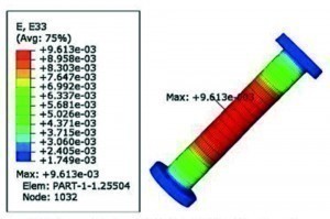 Fig. 4: Remaining stress after three cycles
Aspect ratios of 1:4 do not pose any problems, but when it comes to 1:10, the choice of fab houses is thinned out considerably and 1:15 is probably the end of the line.
If we quickly translate this into actual dimensions, we are talking about an 'aspect ratio' of 1:4 for a 1.60 mm thick PCB with a smallest through-hole of 0.40 mm.
Our engineer mentioned above should also not forget to talk to the assembler, because the specifications for hole diameters depend in part on how the components are threaded. Hand placement is different from machine placement. Good hand placers get the components into much narrower holes than machines, where there are of course also differences. So tolerance calculation is also part of the consideration.
Basically, the hole diameter depends on the wire of the component, if it is not just a matter of changeovers. The thicker the wire, the larger the hole must be. Connectors with many pins require coarser tolerances than components with only two wire connections. Round wires are calculated differently than square or rectangular pins.
Finally, you also want to get solder into the gap and this is where wetting and capillaries come into play again. Solder wets into the through-hole plating, it is not pressed into it, which immediately brings us to the soldering method, the solderability of the PCB and the connecting wires.
Wave soldering is different from selective soldering, which in turn is different from through-hole reflow soldering. Lead-free also throws a spanner in the works, because leaded was not only easier to handle but also wets better due to the overheating (melting point at the eutectic of SnPb approx. 183 °C, soldering temperature approx. 250 °C and therefore an 'excess temperature' of approx. 67 K - melting point of eutectic SnAgCu approx. 217 °C, soldering temperature approx. 265 °C and therefore an 'excess temperature' of 48 K - the situation looks even worse with other lead-free alloys).
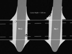 Fig. 5: Pin-in-paste solder joint with few voids - PtH ratio > 0.625 (B. Coleman)
This is related to parameters such as contact time and soldering temperature. We also do not want to ignore the influence of the flux.
Contact times in wave soldering are usually between 3 and 7 seconds. The solder temperature at the peak of the wave is slightly lower than that measured in the crucible itself, and the distance between the preheating and the wave is usually only a few seconds. The entire soldering process is therefore quite well controlled.
Selective soldering depends on the type of machine. If a conveyor belt is used, the assembled component only sees the preheater a few seconds before contact with the solder. However, the chimneys are much smaller and higher and therefore the contact time is shorter. Although they can also be extended by slower transportation, this not only worsens the tear-off, but production also has to accept losses - fewer products fall off the conveyor belt than originally planned.
In selective systems, the solder temperature is also selected differently due to the high chimneys: 285 °C and above does not mean, however, that 265 °C can be measured at the peak of the mini-wave.
If a robot system is used to hold the assembly, the time interval between preheating and soldering is usually longer. If several mini-floods are lowered simultaneously, you occasionally run into coplanarity conditions that can hardly be solved with normal pumps. If you work sequentially, the mini-flood will see a hotter PCB at the first solder joint than at the last. These are all potential wetting problems for the requested through-hole plating.
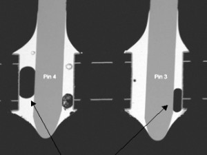 Fig. 6: Pin-in-paste solder joint with voids - PtH ratio < 0.625 (B. Coleman)
Some other, but different, requirements can be found in PiP processes. As paste is printed, the hole size is also important here. Not only the filling is questioned, but also the falling through of the paste, especially with temperature differences and the insertion of the components. If paste is missing, the solder joint is lean.
It is not so much the 'aspect ratio' as the 'pin-to-hole ratio' that has an influence on bubbles and voids in the solder joints, depending of course on the paste used. The ratio of the diameter of the wire to the diameter of the via influences how much gas can accumulate in the solder joint. In such experiments, however, it is not only the paste used that must be taken into consideration, but also the reflow profile, as the viscosity of the molten solder depends heavily on the temperature experienced.
Recommendations to keep the clear width of the vias narrow are based on the difficulty of providing the required amount of metal. However, if this is 'exaggerated', more voids will be found in the solder joint.
Proportions around 0.625 and slightly larger seem to work well in many cases with regard to shrinkage cavities. Below this, there is more air, i.e. gas in the solder joint.
References
- A colloquial, joking comment (especially from craftsmen) when something has been attached, fastened, fitted or installed, not perfectly but successfully. According to www.redensarten-index.de in use from around 1930
- Craig Hillman, Ph.D.¸ Reliable Plated Through Via Design and Fabrication
