For the eleventh time, the Fachverband Elektronikdesign und -fertigung (FED) organized the PCB Designer Day - this year in Leipzig in cooperation with the EMS company beflex/KATEK. The theme of communication ran like a red thread through the event.
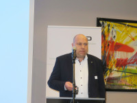
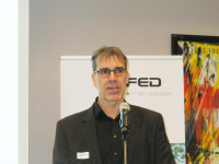
In line with the event motto 'Miniaturization, problem solving and error prevention in PCB design', five specialist presentations and a factory tour were offered. Dieter Müller, Chairman of the FED Board, and Jens Arnold, Managing Director of beflex electronic, opened the 11th PCB Designers' Day, to which they welcomed over one hundred participants.
Jens Arnold introduced the globally active Katek Group and the associated company beflex electronic. Katek employs a total of around 3100 people at 17 locations. The headquarters are in Munich. beflex, headquartered in Frickenhausen, employs 80 people, including 20 project managers. In 2022, the company generated sales of €16 million, 50% of which came from Protoytping. Over 1200 projects are implemented every year. Among other things, beflex offers prototypes in express service from five working days.
Dieter Müller and Jens Arnold concluded by calling for cooperation between EMS companies in order to accelerate developments. "Personal exchange within the design community is extremely important," said Dieter Müller. "The PCB Designer Day offers a platform for this - both for networking and for further training. Practical relevance is important to us. Our speakers are all experienced practitioners. We also give participants the opportunity to visit an electronics production facility. Many designers rarely have the opportunity to do this."
Communication was a recurring theme throughout the event, which was moderated by Michael Matthes, head of the FED Stuttgart regional group. All speakers saw the early exchange between the designer and developers, PCB manufacturers and EMS companies as crucial for successful collaboration in the supply chain.
From prototyping to series production - requirements and challenges
Stefan Burmeister, beflex/Katek, explained how the requirements and challenges can be realized from prototyping to series production. He listed targeted EMS services and used negative practical examples to illustrate the problem of inadequate PCB specifications. Burmeister recommended using the FED document template for the specification of the PCB in the FED knowledge database [1]. This has the advantage that all the parameters required for the manufacture of the PCB are defined. Burmeister used examples from this document to show how detailed it is in the individual specification features. He also discussed possible assembly variants and described the technological process chains required by the design. The design also has to take into account other aspects such as assembly quality, the type of dimensioning of the PCB, the information content of assembly drawings and component tolerances as well as obsolescence management.
PCB design for hearing aids
Kurt Härri (Sonova) dealt with the special challenges of PCB design for hearing aids. Based on an overview of different hearing aid types and their space on or in the ear, he described the design requirements: Many components with little space on the circuit board, influences of heat and humidity as well as the acoustic requirements and low available energy. Härri showed how these pitfalls can be avoided with creative approaches in the design of flex PCBs. He also emphasized the importance of communication between developers and designers in order to keep the number of necessary design iterations to a minimum.
All in - miniaturization with embedded components
Michael Schwitzer (Ciboard) used the example of control electronics for an e-cigarette to show how to get started with embedded component technology. He explained in detail how the project was carried out, from the inquiry and clarification of the design task and the framework conditions to the selection of EC technology, implementation in the printed circuit board and assembly and testing. Solder embedding was selected as the EC technology and the design was carried out using the EDA system. All mechanical and design requirements were successfully implemented through the use of embedded and HDI technology and close coordination with the PCB manufacturer from the outset. Ciboard received the PCB Design Award for this last year.
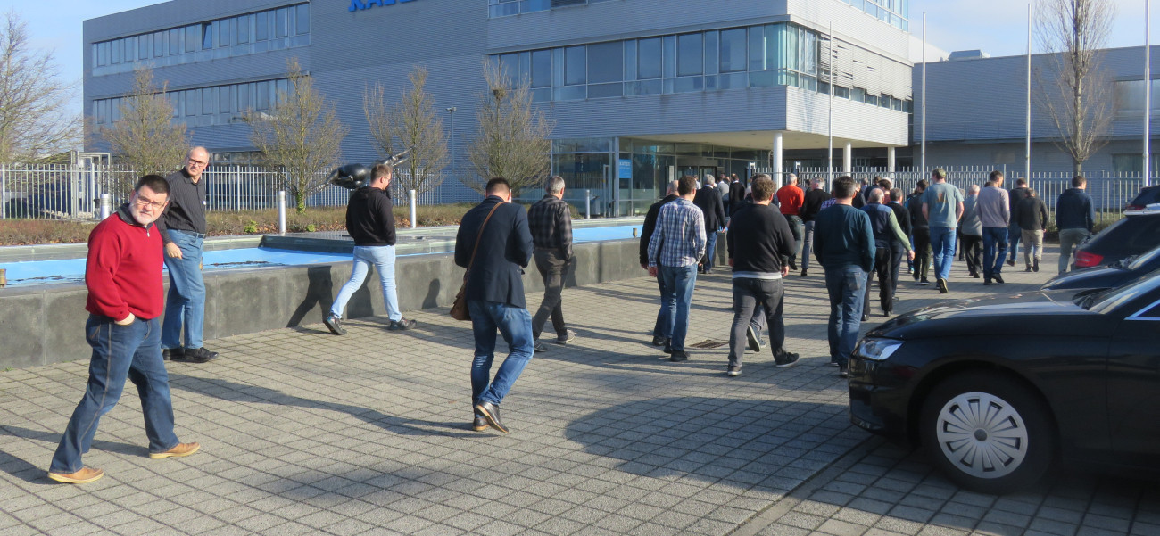 At the start of the factory tour at KATEK Leipzig
Layout creation only a matter of design - practical approaches to avoiding errors
Bernd Lauterwasser (beflex/Katek) addressed the quality of design creation. Using practical tips and numerous concrete examples, he explained how costly errors in PCB design can be avoided from the outset. In conclusion, he gave the tip to talk to the developer, the PCB manufacturer and the component manufacturer at an early stage and to find a good compromise together.
Novel applications in the PCB and their implementation with EDA tools
In the last presentation, Michael Matthes (Würth Elektronik) provided information on innovative PCB applications. He began by discussing the new classification model created by the FED for PCB additive technologies. He presented the digital solder mask (s.mask) and the stretchable PCB (stretch.flex) as examples of new technologies at the PCB manufacturer. Matthes explained the advantages of these technologies in detail and also went into the possibilities of the EDA tools. The digital solder mask is applied by inkjetting only where it is needed. Different thicknesses can be realized and the LSM can also be applied in cavities. EDA tools enable manual application of the digital solder mask to each individual layer as well as automatic application per region and per type/geometry. For stretch.flex, thermoplastic polyurethane is used as a carrier material with laminated copper. The conductor structures are designed in a meander shape to achieve stretchability. Otherwise, established manufacturing processes can be used and there are a wide range of further processing options. The first design tools offer different meander structures (full arc, snake, triangular and square) and the complete design is provided with the previously selected meander structures at the touch of a button.
Factory tour - a highlight at the end
After the lecture program, we went on a two-hour factory tour. The Leipzig site has been part of the Katek Group since 2021. Formerly known as Leesys, the company now specializes in the development and manufacture of electronic assemblies. Five groups - led by the experts - visit the warehouse, SMT, THT, test, assembly, plastic injection molding and beflex plant areas. A special feature of the plant is that the entire material transport from the warehouse to and between the workstations and back is fully automated using robotic vehicles.
The next PCB Designer Day will take place on February 27, 2024 in Niedernhall in cooperation with Würth Elektronik.
References
[1] See document 2022-03-22_FED_template_PCB_specification_V1.4.dotx in: www.fed.de/wissensdatenbank


