Due to the increasing amount of electronic waste (e-waste) worldwide, the disposal of waste printed circuit boards (WPCB) has become a major environmental challenge. This paper presents a new composite material for the production of printed circuit boards that can be easily converted back into its original components, making them reusable.
Due to the ever-increasing amount of electronic waste (e-waste) worldwide, the disposal of printed circuit boards waste (WPCB) has become a major environmental challenge. This paper presents a new composite material for the manufacture of printed circuit boards (PCB) that can be easily recycled into their original components and reused.
1 Introduction
The rapid increase in the use of electronics in a wide range of sectors, including consumer goods and industry, has led to a steady increase in the production of printed circuit boards. Ultimately, this has led to a steady increase in the amount of electronic waste [1]. According to statistics, more than 50 million tons of electronic waste are generated worldwide every year, with up to 10 percent of this mass being old printed circuit boards [2].
The PCBs traditionally used in the electronics industry consist of a dielectric composite material that serves as a mechanical carrier for the components and conductor tracks. The latter are usually produced by etching copper foils that are laminated onto one or both sides of the dielectric base. These in turn consist of several layers of glass fabric or paper, which are impregnated with thermosetting resin as a binder and then formed in a hot press [3].
Currently, highly toxic raw materials (epoxy and phenol-formaldehyde resin and their mixtures; combined epoxy-silicone resin; combined epoxy-polyimide resin, bismaleimide resins, triazine resin, etc.) are used as binders. These resins come from non-renewable sources. In addition, boards made from such resins are not degraded by microorganisms under environmental conditions, which contradicts today's requirements for the safety of chemical processes and materials [4]. WPCBs, with their metallic (approx. 30 % by weight) and non-metallic (approx. 70 % by weight) fractions, are the most difficult components of electronic waste to recycle - although they contain both hazardous and valuable components [5, 6].
Despite the wide range of applications of printed circuit boards - from cell phones and household appliances to automobiles and industrial process controls - WPCBs are characterized by a relatively high content of precious metals such as Pd, Au, Pt, Ag and base metals such as Cu, Fe, Ni, Zn, Sn, Pb. In addition, the amount of metal can vary more than tenfold even for one and the same product type (e.g. cell phones) [7]. From an economic point of view, the recovery of precious metals is very promising, as each ton of WPCB contains on average 130 kg of copper, 1.38 kg of silver, 0.35 kg of gold and 0.21 kg of palladium, and the precious metals can account for more than 80% of the economic value [8].
Today, WPCB recycling is mainly aimed at recovering metals with high added value, while the non-metallic fraction is usually landfilled or incinerated without further recycling. The non-metallic WPCB fraction contains toxic resins and brominated flame retardants [9], which are extremely hazardous compounds that affect human health and are considered to cause cancer [10, 11]. It should be mentioned that toxic WPCB compounds can easily leach from landfills into groundwater, resulting in long-term contamination of large areas [12]. The above threats have led to an active scientific search for WPCB disposal and recycling methods.
The rapid development in the synthesis and production of new biodegradable polymers is currently stimulating scientists to develop new types of binders for PCBs produced from renewable resources using biotechnological and chemical processes [13]. In particular, the investigation of biodegradable polymers is attracting particular interest due to their increasingly diverse applications. Biodegradable polymers are widely used in the packaging industry and in medicine and their practical fields of application are expanding considerably [14-16].
Polymers based on polylactic acid (PLA) and copolymers of PLA with other hydroxycarboxylic acids are thermoplastic polymers with mechanical and electrical properties close to those of thermoset resins, but at the same time these materials can be easily recycled for reuse by chemical and biotechnological processes [17].
In this work, a new approach to use biodegradable polymers as binders for printed circuit board manufacturing is presented. The use of biodegradable and easily recyclable polymers as binders opens up new perspectives for both environmental protection and resource conservation and aims to maximize the recovery of valuable materials for their reuse.
2 Results and discussion 2.1 Production of a double-sided metallized printed circuit board and assembly of electronic components
To produce the prepreg (composite PCB backbone), PLA was dissolved in chloroform at 75-80 °C and a molar ratio of PLA to chloroform of 1:3. The solution was prepared in a reflux condenser with constant heating and stirring on a magnetic stirrer at 200 rpm. Then, glass fabric sections with a size of 60 mm×110 mm were dipped into the obtained solution and dried at room temperature in a chemical oven for two hours. The density of the prepreg obtained was 110-140 g/m2. To produce a printed circuit board, six layers of prepreg were stacked on a Teflon-coated metal mold. The copper foil was placed on the top and bottom of the prepreg stack. The mold was then sealed with a metal plate (100 mm × 120 mm) and also covered with Teflon to prevent the composite material from sticking to the mold. The mold was then placed in a hot press and heated to 195 °C. After the prepreg had five minutes to soften, a pressure of 0.2 MPa was applied to the mold for one minute. The mould was removed from the press and after cooling to room temperature, the double-sided metallized PCB with a thickness of about 1 mm could be removed from the mould(Fig. 1a).
A special marker (Edding 780) was used to mark the conductor tracks on the copper-clad carrier. The excess copper foil was etched away in iron(III) chloride solution (500 g/L) at 50 °C for 20 min. After the etching process, the marker traces were thoroughly removed with ethanol. The final result was a printed circuit board with conductive copper tracks(Fig. 1b). The electronic components (chips, LEDs, capacitors and resistors) were then soldered onto the circuit board using a Rose alloy (melting point 95 °C)(Fig. 1c). The reason for choosing the Rose alloy was that at soldering temperatures above 120 °C the copper tracks sometimes peeled off the laminate.
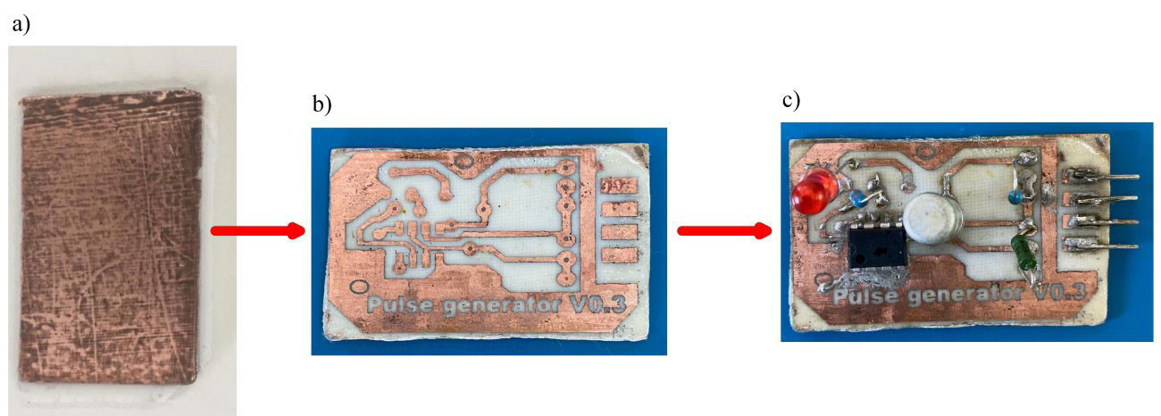 Fig. 1: Board production and installation of the electronic components: a) double-sided metallized circuit board produced in the laboratory, b) circuit board with copper conductor tracks, c) electronic assembly produced in the laboratory
2.2 Measurement of the dielectric, thermal and mechanical properties of PLA PCBs
Printed circuit boards used in the electronics industry are subject to different requirements depending on the area of application. The list of the most important properties of a laminate made of composite materials includes parameters such as volume resistivity, dielectric loss factor, dielectric permittivity, glass transition temperature, tensile strength and flexural strength. In order to compare the electrical properties of the most common commercial printed circuit boards (FR2, FR4) and the PLA printed circuit boards produced in the laboratory, corresponding comparative measurements of the properties were carried out. The results are shown in Figure 2.
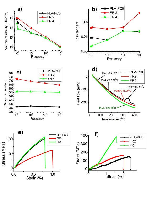 Fig. 2: Results of the parameter measurements of three PCB types: a) electrical volume resistance b) dielectric loss factor c) dielectric permittivity d) thermogravimetric differential calorimetry e) tensile strength and f) bending testAbrief comparison of the main dielectric, thermal and mechanical properties of PLA-PCB and commercial PCB samples is shown in Table 1.
|
Material parameters |
Material unit |
PLA-PCB |
FR2 |
FR4 |
|
Volume resistance at 105 Hz |
Ohm*m |
1,12.103 |
1,22.103 |
0,79.103 |
|
Dielectric loss factor at 105 Hz |
- |
2,89.10-2 |
4,37.10-1 |
2,42.10-2 |
|
Dielectric permittivity at 105 Hz |
- |
3,66 |
6,46 |
5,51 |
|
Glass transition temperature Tg |
0C |
83,1 |
65 |
134,5 |
|
Ultimate tensile strength |
MPa |
102,3 |
61,9 |
108,1 |
|
Ultimate flexural strength |
MPa |
147,6 |
162,4 |
321,5 |
The results show that the experimental values of specific volume, loss tangent values, dielectric permittivity, glass transition temperature, tensile and flexural strength of PLA-PCB are generally similar to those of commercial FR2 and FR4 samples:
- The contact resistance of PLA-PCB at 105 Hz is higher than that of FR2 and lower than that of FR4
- The tangential loss values of PLA-PCB at 105 Hz are lower than FR2 and almost the same as FR4
- The dielectric permittivity of PLA PCBs at 105 Hz is lower than that of commercial PCBs
- The glass transition temperature of PLA-PCB is between the values of FR2 and FR4
- The tensile strength of PLA-PCB is higher than in the case of FR2 and practically equal to the tensile strength of FR4
- The final flexural strength of PLA-PCB is lower than that of FR4 and slightly lower than that of FR2
In our opinion, the lower final flexural strength is due to the fact that the number of glass fiber layers in FR4 is more than 8, while the PLA-PCB contains only 6 layers of glass fiber fabric.
2.3 Recycling of a printed circuit board produced in the laboratory
The recycling process for PCBs produced in the laboratory is shown in Figure 3. For sample recycling, the PLA PCB(Fig. 3a) was placed in a container with the solvent tetrahydrofuran and then placed in an ultrasonic bath. This process allowed a complete separation of the binder (PLA), the copper tracks with electronic components and the filler (glass fiber) from each other without additional manual [18], mechanical and thermal processes [19]. The process of recycling electronic assemblies was completed within 30 minutes. The PLA solution in the tetrahydrofuran could be evaporated to dryness in a rotary evaporator in a vacuum at a water bath temperature of 40 °C, whereby 98 percent by weight of the PLA was recovered(Fig. 3e).
After recycling, only the copper sheets(Fig. 3c) with electronic components(Fig. 3b) and glass fiber layers(Fig. 3d) remained in the container. The figure shows the electronic components after they have been separated from the copper tracks.
Previously, an article in [20] demonstrated the possibility of PLA-PCB recycling under extraction conditions in a Soxhlet apparatus, in which ethyl acetate dissolved the PLA and separated it from the filler and copper traces. Despite the promising results, the fundamental disadvantages of recycling using Soxhlet extraction are the time and energy consumption. In contrast, PLA-PCB recycling using ultrasound is twice as fast as in the Soxhlet apparatus [20] and energy efficient. It should also be noted that, in contrast to Soxhlet extraction, the ultrasonic method does not require running water for cooling.
It is noteworthy that the marking and protective layers on the microchip, resistors or capacitors did not disintegrate and their electrical properties were completely intact(Fig. 3b), which allows the use of expensive electronic components for their entire life cycle.
Tetrahydrofuran was recovered after the PLA-PCB recycling process by solvent distillation on a rotary evaporator under vacuum in a water bath. After solvent distillation and vacuum drying, the PLA was extracted(Fig. 3e).
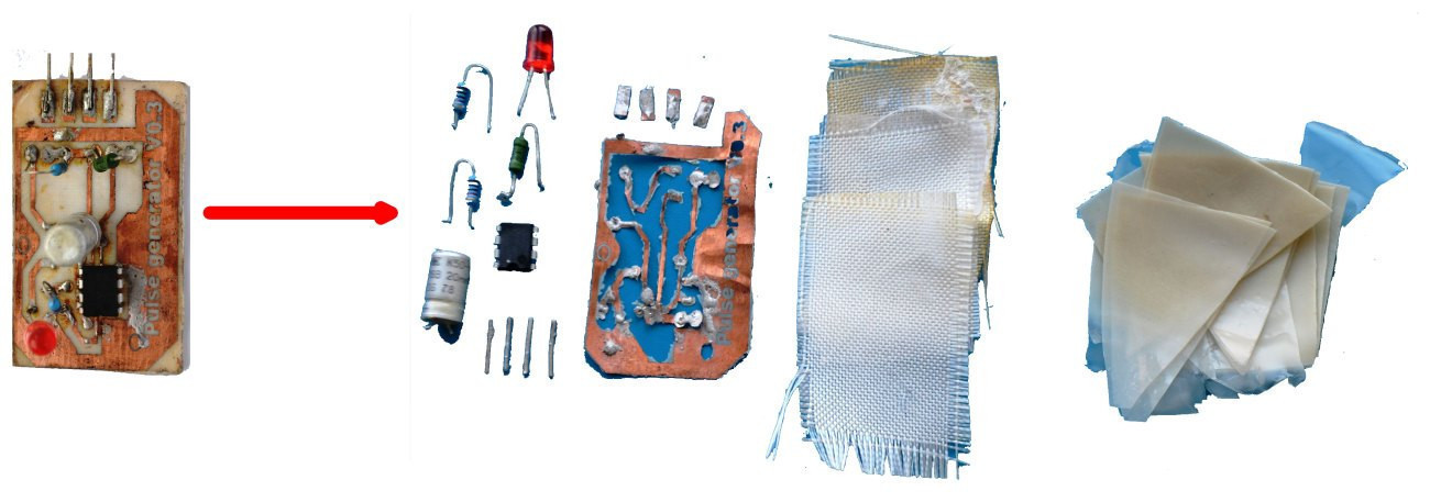 Fig. 3: Recycling of PLA-PCB: a) PLA-PCB produced in the laboratory, b) electronic components, c) copper conductor, d) glass fiber layers, e) polylactic acid after the recycling processIn order toinvestigate the complete dissolution of the PLA, the glass fiber surface was examined with a scanning electron microscope. Figure 4 shows SEM images of the original fiberglass(Fig. 4a) and the fiberglass after recycling(Fig. 4b). After recycling, the binder (PLA) dissolved completely and the fiberglass fabric was intact. Even after being recycled three times, the fiberglass remained intact(Fig. 4c), which indicates a high probability of reuse. In contrast, the fiberglass is damaged by thermal, mechanical and chemical processes in traditional WPCB recycling techniques. It can then only be reused as a reinforcing filler in bricks for the construction industry, for example [21].
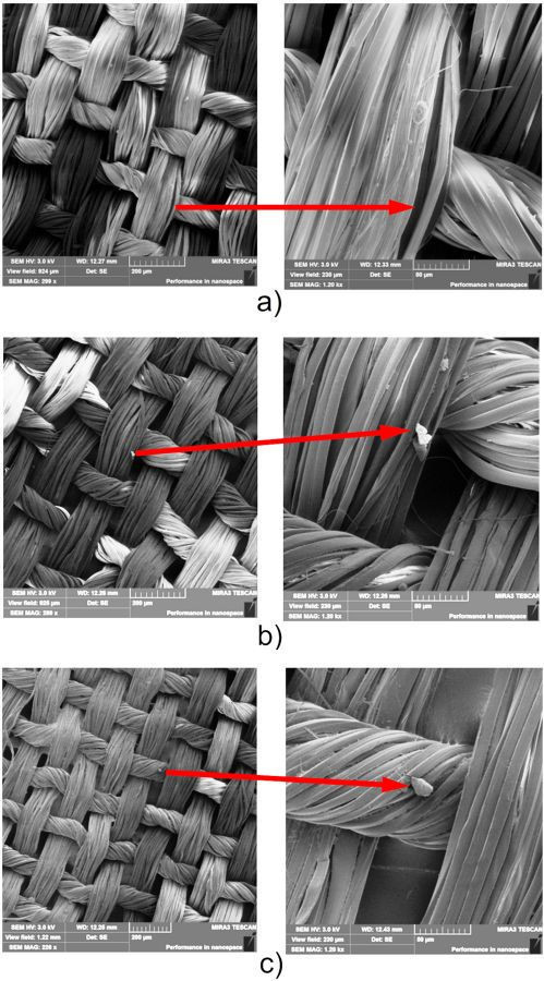 Fig. 4: SEM images of PLA glass fabrics: a) Original glass fabric used for the production of PLA printed circuit boards b) Glass fabric after single recycling c) Glass fabric after triple recycling
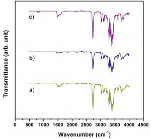 Fig. 5: FTIR spectra of PLA: a) starting material; b) reconstituted once and c) three times from recycled PLA PCBsToinvestigate the influence of PLA-PCB recycling and subsequent extraction on the structure of PLA, FTIR (Fourier transform infrared spectrometer) spectra of primary PLA and recovered PLA-PCB were analyzed(Fig. 5). The PLA shows characteristic stretching frequencies for C=O, -CH3 asymmetric, -CH3 symmetric and C-O at 1746, 2995, 2946 and 1080 cm-1, respectively.
The bending frequencies for -CH3 asymmetric and -CH3 symmetric were identified at 1452 and 1361 cm-1, respectively. The PLA recovered after single(Fig. 5b) and triple(Fig. 5c) recycling of PLA-PCB shows the same absorption peaks as the original PLA(Fig. 5a). Thus, the binder (PLA) was not chemically degraded during either the production or recycling of PLA-PCB and can be reused for PCB production.
Overall, after the recycling process of the PLA PCBs produced in the laboratory, 95 % of the weight of the binder (PLA), 100 % of the weight of the filler (glass fiber), 100 % of the electronic components and 100 % of the copper conductors were recovered for reuse. According to average estimates, more than 50 million tons of electronic waste are produced worldwide each year, with WPCBs accounting for between 3-10% of this amount by weight [2].
Taking into account the average Cu content in WPCBs, it can be estimated that around 195,000 to 650,000 tons of copper are recycled or landfilled annually. In the case of 100% copper recycling with WPCBs, the economic effect would be between 1.6 and 5.38 billion US dollars per year.
The difference between laboratory-produced PLA PCBs and PCBs currently manufactured on an industrial scale (e.g. FR2 and FR4 [22]) is that toxic and difficult-to-recycle binders based on epoxy and phenol-formaldehyde resins could be replaced by an environmentally friendly and easily recyclable PLA-based binder.
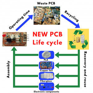 PLA-PCB life cycle as defined in the studyThecost of the binder currently used in the industry to manufacture commercial printed circuit boards varies between 4.3 and 4.7 US dollars per kilogram [23]. The cost of PLA is also between 0.94 and 3.3 US dollars per kilogram [24]. Therefore, the cost of binders currently used in PCB manufacturing and the cost of PLA are in the same price range, and the use of PLA as a binder for PCB manufacturing will not increase the cost of the final product.
In addition, a PLA-based PCB offers complete recovery of raw materials and chemicals after the recycling process, which is currently not possible with conventional PCBs [25]. An important advantage of the proposed PLA-PCB is that the PLA-based binder will biodegrade without contaminating the environment with decomposition products if it ends up in a landfill [1].
Summary
A new process for the production and recycling of printed circuit boards using PLA as a binder for efficient and environmentally friendly recycling of WPCB has been proposed. The novelty of the process is to replace the toxic and difficult-to-recycle thermosetting resins currently used for PCB manufacturing with PLA, which is biodegradable and easily recyclable. The study found that PLA PCBs can be easily recycled back to their original components. Ultimately, after recycling the PLA PCBs produced in the laboratory, more than 95% of the weight of the raw materials and 100% of the electronic components were recovered for reuse. The PCB industry is currently based on the overuse of non-renewable resources and is characterized by low recycling of WPCBs, which does not comply with the principles of a sustainable economy and ultimately increases the final price. From this point of view, the gradual conversion to renewable raw materials in the production of commercial printed circuit boards and the implementation of processes for their easy recycling can have a positive impact on the conservation of valuable non-renewable resources and the possibility of their reuse. Implementing the production and recycling of PLA PCBs as proposed in this article could bring the PCB industry much closer to adopting a circular economy.
Created under the Creative Commons License CC BY 4.0
Translation: Dr. Ing. Hartmut Poschmann
Acknowledgments: This work was supported by the Public Association RK 'Green Chemistry'. For further information, please visit the following website: http://greenchemistry.kz/
Note from the translator:
The bibliography contains numerous current publications on PCB recycling and gives interested parties an impression of the diversity of work on this important topic. It is remarkable that solutions to the PCB recycling problem are being worked on in many parts of the world, even in Kazakhstan, which seems so far away to us.
References
[1] Forti, V. et al.: The Global E-waste Monitor 2020: Quantities, flows and the circular economy potential, United Nations University (UNU)/United Nations Institute for Training and Research (UNITAR)-co-hosted SCYCLE Programme, International Telecommunication Union & International Solid Waste Association, 2020
[2] Kaya, M.: Electronic waste and printed circuit board recycling technologies in The Minerals, Metals & Materials Series, 326 P., Springer, Cham, 2019
[3] Stevens, G.C.; Goosey, M.: Materials used in manufacturing electrical and electronic products in Electronic Waste Management (ed. Hester, E. & Harrison, R. M.) Royal Society of Chemistry, Cambridge, 2009, 33-35
[4] Anastas, P.T.; Warner, J.C.: Green Chemistry: Theory and Practice, Oxford University Press, 1998
[5] Rajagopal, R. et al: Activated carbon derived from non-metallic printed circuit board waste for supercapacitor application, Electrochim. Acta 211, 2016, 488-498.
[6] Wang, J.; Xu, Z.: Disposing and recycling waste printed circuit boards: disconnecting, resource recovery, and pollution control,Environ. Sci. Technol. 49,2015, 721-733
[7] Sahan, M. et al: Determination of Metal Content of Waste Mobile Phones and Estimation of Their Recovery Potential in Turkey, Int. J. Environ. Res. Public Health 16, 2019, 887
[8] Hagelüken, C.: Improving metal returns and eco-efficiency in electronics recycling-A holistic approach for interface optimization between pre-processing and integrated metals smelting and refining IEEE International Symposium on Electronics and the Environment, Proceedings of the IEEE International Symposium on Electronics and the Environment, 2006, 218-223
[9] Kovačević, T. et al: New composites based on waste PET and non-metallic fraction from waste printed circuit boards: Mechanical and thermal properties, Compos. B. Eng. 127, 2017, 1-14
[10] Wemken, N. et al.: Concentrations of brominated flame retardants in indoor air and dust from ireland reveal elevated exposure to decabromodiphenyl ethane, Environ. Sci. Technol. 53, 2019, 9826-9836
[11] Gómez, M. et al: Stabilization of hazardous compounds from WEEE plastic: Development of a novel core-shell recycled plastic aggregate for use in building materials, Constr.Build.Mater. 230, 2020, 116977
[12] Ogunseitan, O.A.: The Basel Convention and e-waste: translation of scientific uncertainty to protective policy, Lancet Glob.Health 1, 2013, 313-314
[13] Feig, V.R. et al: Biodegradable polymeric materials in degradable electronic devices, ACS Cent. Sci. 4, 2018, 337-348
[14] Li, R. et al: Materials and devices for biodegradable and soft biomedical electronics, Materials 11, 2018, 2108-2131
[15] Hwang, S.-W. et al: Biodegradable elastomers and silicon nanomembranes/nanoribbons for stretchable, transient electronics, and biosensors, Nano Lett. 15, 2015, 2801-2808
[16] Kook, G. et al: Wafer-scale multilayer fabrication for silk fibroin-based microelectronics, ACS Appl. Mater. Interfaces 11, 2019, 115-124
[17] Rydz, J. et al: Present and future of biodegradable polymers for food packaging applications in Handbook of Food Bioengineering (ed. Grumezescu, A. M. and Holban, A. M.) Academic Press, 2018, 431-467
[18] Copani, G. et al: Integrated technological solutions for zero waste recycling of printed circuit boards in Factories of the Future (ed. Tolio, T., Copani, G. & Terkaj, W.) Springer, Cham., 2019, 149-169
[19] Kaya, M.: Recovery of metals and nonmetals from electronic waste by physical and chemical recycling processes. Waste Manage. 57, 2016, 64-90
[20] Yedrissov, A.; Khrustalev, D. et al: New composite material for biodegradable electronics, Mater. Today: Proc. 49, 2022, 2443-2448
[21] Kovačević, T. et al.: Effects of oxidized/treated non-metallic fillers obtained from waste printed circuit boards on mechanical properties and shrinkage of unsaturated polyester-based composites, Polym. Compos. 40, 2019, 1170-1186
[22] Sarvar, F. et al: PCB glass-fiber laminates: Thermal conductivity measurements and their effect on simulation, J. Electron. Mater. 19, 1990, 1345-1350
[23] Why printed circuit board prices go up in 2021? https://www.pcbonline.com/blog/why-do-printed-circuit-board-prices-go-up.html, 2021
[24] Wellenreuther, C. et al: Cost competitiveness of sustainable bioplastic feedstocks - A Monte Carlo analysis for polylactic acid, Cleaner Engineering and Technology 6, 2022, 100411
[25] Rocchetti, L. et al: Printed circuit board recycling: A patent review, J. Clean. Prod. 178, 2018, 814-832


