
More and more electronic assemblies are taking over vital functions, for example in electronic braking systems. This leads to ever higher demands on the quality of the products, as an electronic braking system should protect our lives in an emergency and not pose an additional threat. This means that the quality of a solder joint must be determined beyond doubt by measurement and documented with all its geometric properties for traceability.
As we have already seen in 3D solder paste inspection, the increased requirements in solder joint evaluation have helped 3D measurement technology to make a breakthrough. More and more suppliers are trying to jump on the 3D bandwagon, so that the market is currently flooded with 3D systems.
Users are inundated with a mass of marketing materials and specifications. It is difficult to differentiate between machines on the basis of data sheets alone. So you need a solid performance comparison to help you decide. Where are the limits of the new machines? Which errors, component sizes and distances can still be measured reliably? How much time do you need to spend on program creation and adaptation, i.e. debugging? How repeatable is the measurement? Do the layout and orientation of the components have an influence? Is it possible to inspect according to IPC classes? It quickly becomes clear that the task of a proper machine comparison is not an easy one.
This makes the right choice of a suitable test assembly all the more important. Unfortunately, this is not always available at the right moment:
- Production PCBs are not suitable because they do not represent the limits of what is feasible, as they were designed for production with little variation.
- Demonstration PCBs from manufacturers are also unsuitable, as they usually demonstrate what the manufacturer can do and not what it cannot do.
- Another problem arises when mapping the 3D measurement. Many test boards address the requirements of 2D inspection, i.e. a "defect image" is checked. In a 3D measurement, however, heights and volumes are "measured". Different heights and volumes are therefore required here to define the limit of what can be detected. The failure criterion is a value. A test and benchmark board must therefore offer the possibility of testing with different failure values.
- Developing your own demonstrator is costly and time-consuming, and a certain amount of experience is also required to reproduce errors realistically.
In response to this need, Koh Young teamed up with Hannusch Industrieelektronik and Christian Koenen GmbH a few years ago to jointly develop a benchmark board that also meets the requirements of a 3D measurement. This is how the first "qualification board" was created.
Over time, the initial self-help project developed into a product that is already in its 9th generation of production. In the meantime, a larger group of cooperation partners from the SMT world is supporting production with specialist articles, materials and a wealth of expertise. You can see the result in the design of the current KYv9 qualification board, or in the many technical articles in our booklet "Koh Young Test & Benchmark Board Version 9", which is now in its 5th edition.
But what is behind the promising name "Qualification Board"?
The board design
Challenging layouts have been developed using the experience of users and programmers from the 2D AOI world. For example, the pad spacing and sizes are varied for the same designs, because the production reality with poor layouts and etching tolerances of the PCBs should be simulated as closely as possible. If the test algorithms are based on image comparisons, difficulties will arise when assigning identical components. This allows four comparisons to be mapped:
- Whether the AOI uses image comparison (2D) or a measurement method (3D).
- How much effort is involved in optimizing the inspection program (debugging).
- Does the inspection system react sensitively to inter-reflections between neighboring solder joints.
- Can the test system resolve small component distances.
 Figure 1: Different pad sizes and distancesTheboard has a representative cross-section of designs that can still be sensibly combined in one design. This is why the smallest chip size was limited to 01005. In total, there are just over 1,500 small to large components on the board.
Larger components can make it difficult or even impossible to inspect other components due to shadowing. This quickly reveals the limits of side camera technology. In addition, the component mix shows how well an AOI can illuminate these shadow areas with its lighting options and how the algorithms process the interference signals.
Reflections represent a white spot in the measurement. Image information is simply blended over. This happens quickly when measuring reflective surfaces or white components. Both aspects are taken into account by suitable components.
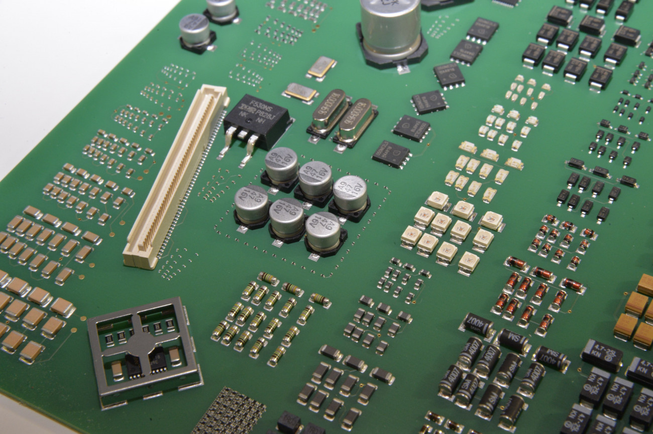 Figure 2: Component mix
 Figure 3: Shadow scenario example
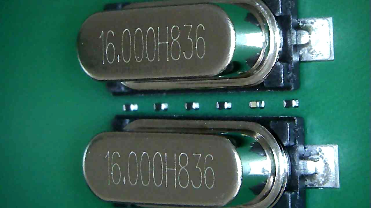 Fig. 4+5: Reflective components and white LED
Manipulated faults
Not all faults can be realized via the PCB layout. Therefore, the production and the material can be manipulated in a targeted manner.
1. printed defects (stencil manipulation)
Offset and volume errors are generated via the stencil layout. In this way, the different IPC classes can be mapped for the chip components, BGAs can be soldered at an angle and tombstones and solder beads can be created.
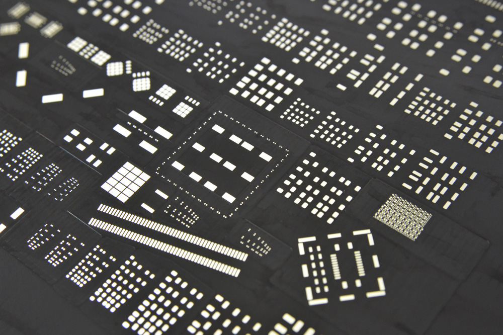 Figure 7: Stencil...
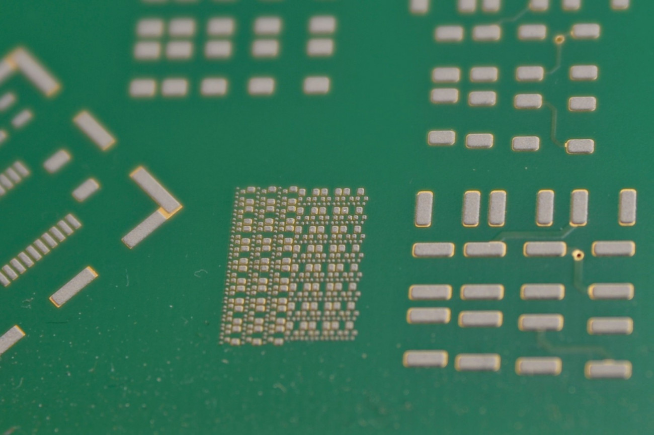 Figure 8: ...and print result
2. assembled errors (placement manipulation)
Component rotations, offsets, polarity errors, incorrect placement and "dropped components" can be realized with the placement. Specially taped SOTs are assembled upside-down.
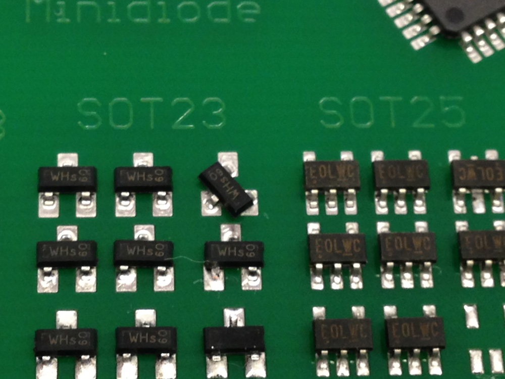 Figure 9: Placement errors (center rotation, bottom center upside-down, top right 180° rotated, bottom right missing)
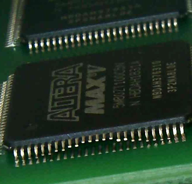 Figure 10: Lifted lead error
3. manipulated components
Lifted-lead faults are created on QFPs using specially manufactured bending tools.
If the most stringent inspection criteria are selected, including IPC soldering class testing, up to 1,200 defects can be detected in a 100% inspection. It's easy to lose track. This is why all manipulations and the resulting faults are documented.
Why the effort?
It is about the comparability of optical measuring systems. This also includes knowing the limits of the optical inspection systems and revealing differences in the inspection philosophy and measurement concepts. None of this is possible by comparing data sheets. Ordinary assemblies and demonstration boards contain too few extremes and no structures for variable design of the failure criteria, such as linearly increasing lifted-lead defects. A benchmark board is therefore essential for the value-free comparison of AOI systems.
 Fig. 11-13: Examples of 3D measurement (from left: billboard error, joint measurement, 3D polarity marker)What does 3D mean from the perspective of the individual AOI providers?
- Does 3D mean 100% 3D measurement or as required?
- Does 3D mean only planarity or 100% component and solder joint inspection?
At this point, the term 3D is very overused. A benchmark board will show the differences transparently.
3D solder joint inspection also means measuring a solder joint with volume, wetting height, lead height and position under adverse conditions: Reflections, reflective surfaces, measuring smoke from neighboring solder joints, curved PCBs and much more. The quality of the 3D measurement is demonstrated in this harsh environment.
A benchmark board that maps the various solder volumes and generates reflections from neighboring components and solder joints is helpful here. Different lead heights can also be measured via the manipulated components. Ideal for determining repeatability and measurement accuracy or linearity comparisons.
 Figure 12
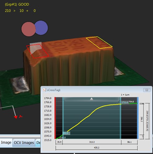 Figure 13
A world of light and shadow
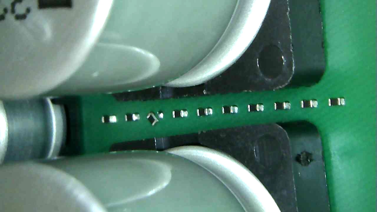 Figure 14: Shadow problemThelayout of a PCB does not take into account the requirements of an optical inspection. Although AOI manufacturers make repeated efforts to provide design recommendations, in reality the design and layout are determined by the electrical and mechanical functions and the available space. In order not to deprive yourself of all flexibility in production in advance, you should consciously create and test the shadow scenarios. A benchmark board generates these critical layout scenarios.
The shadows also occur with small components in dense placement. Therefore, the number, arrangement and projection angle of the light sources are important factors for a shadow-free measurement.
A benchmark board helps to work out the differences between the AOIs at this point. If, for example, the assembly is inspected with different rotation angles, the rotation test shows the differences in the light sources.
Position determination
As a general rule, determining the position via the component body is more accurate. This is because it is difficult to determine the start and end of a component contact depending on the solder volume. The AOI providers also differ here. In the 2D world, the position was determined via the detected component connections. This has been adopted by many providers in the 3D world. However, the contours of a component connection that is completely covered with solder are difficult to interpret. A benchmark board offers different solder volumes for the same designs. This allows the robustness and stability of the position measurement to be verified using repeat measurements.
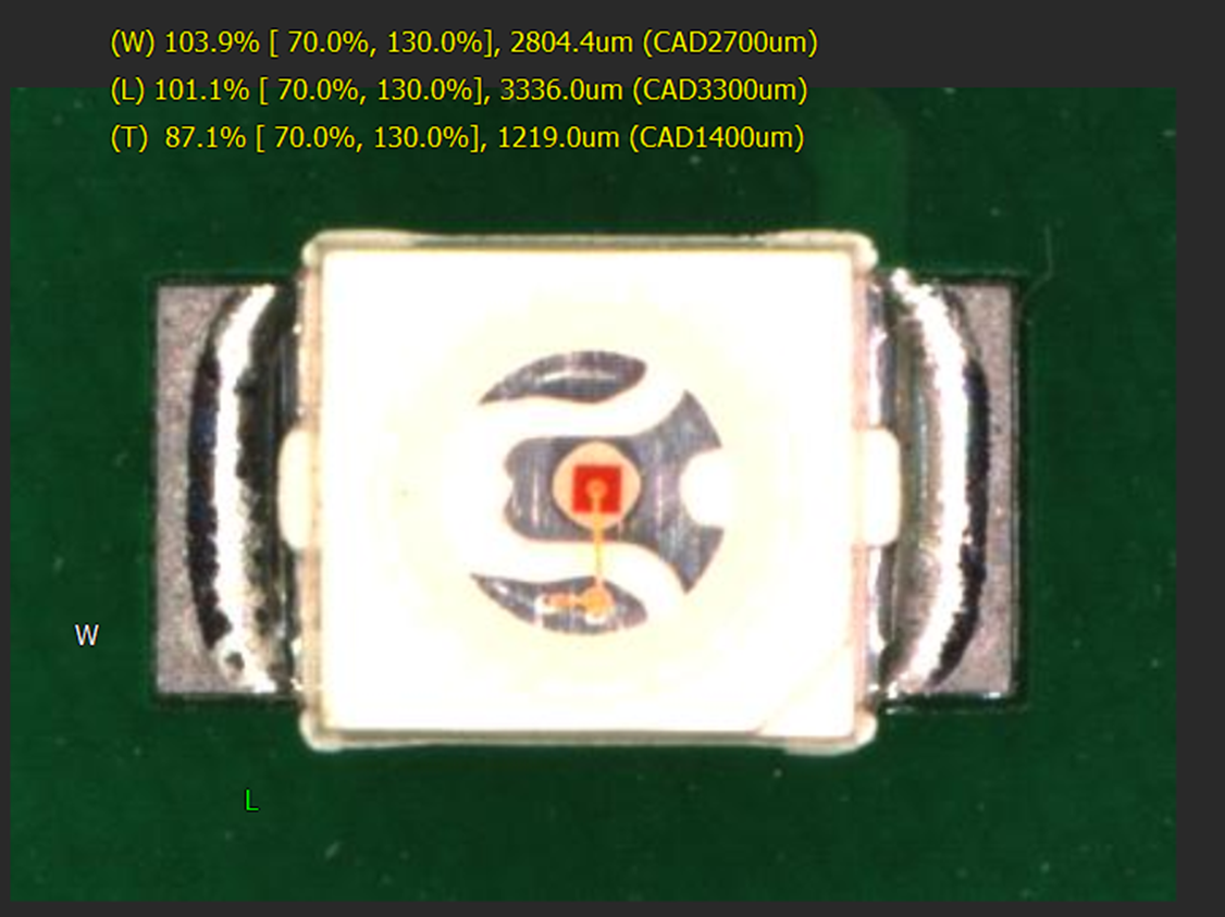
 Figure 15: Example of 3D LED measurementThepositioning of an LED quickly becomes a decisive quality criterion, as the angle and position of the light source make a decisive contribution to its function. With a 100% 3D measurement, the polarization marks and the component body can be determined clearly and precisely even on a white LED. As the phosphor chip under the LED lens itself has positional tolerances to the LED housing, the position and alignment of the phosphor chip is also measured. The benchmark board therefore has a number of white LEDs with corresponding measurement options.
These are just a few examples from the layout of the current qualification board. They are intended to show you the advantages and benefits of a well thought-out test and benchmark board.
A benchmark board can never cover all applications and fault patterns. Nevertheless, we try to represent as many error types and challenges as possible. A benchmark board, such as the KYv9 qualification board, can be a useful tool for orientation. In a world of glossy brochures, marketing promises and barely distinguishable specifications, it gives us a clear picture based on solid measurement results. The many scenarios show us not only the limits of optical inspection, but also the possibilities of finding the right solution for difficult situations. A benchmark board can also quickly become a test and training board for algorithms and employees.
This is why Koh Young and its partners are constantly developing new generations of the qualification board with new challenges for all optical measurement systems. Our ideas are based on our experience and the applications of our customers.
By the way, the qualification board is also a challenge for Koh Young and we are also reaching our limits.
But it's best to find out for yourself.
