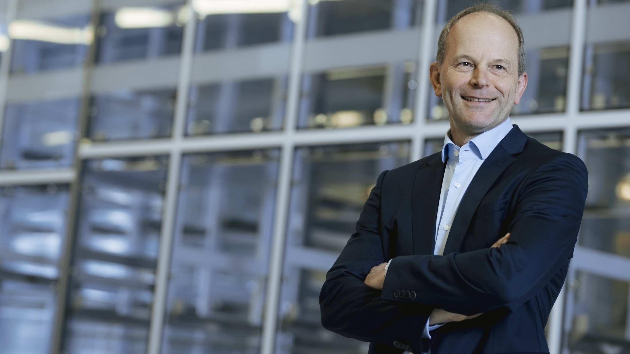
AT&S is making great strides from its original PCB manufacturer to become a versatile AVT specialist in microelectronics. To this end, the company is investing in a new R&D center at its headquarters in Leoben (Austria), as well as production expansions for small series and prototypes. A total of up to 700 new jobs will be created. The investment sum planned for the coming years up to 2025 amounts to €0.5 billion - this also includes funding from IPCEI2. CEO Andreas Gerstenmayer at the presentation of the investment project last Friday: "Moore's Law is exhausted in its basic idea, which is why so-called backend services are becoming increasingly important." In other words, semiconductor development on silicon alone can no longer deliver the performance increases required in the future as usual - AVT further developments, embedding and other technological combination approaches of silicon and PCB are required here. To date, the main players in these back-end services have been based in Asia - with 50% of the global market share in Taiwan and 20% in the People's Republic of China. "Backend services still take place a little in the USA, but there are practically none in the EU," says Gerstenmayer.
Because the Austrian company's investment plans fit in with current geostrategic necessities and the EU funding programme IPCEI2, Margarete Schramböck, the Austrian Federal Minister responsible for digitalization and location policy, also spoke at the press conference. She cited the AT&S project and the opening of Infineon's power semiconductor chip factory in Villach in mid-September as strategically important examples of "investments in modern, digital key industries that provide jobs, enhance regions and thus strengthen the location in the long term. We have succeeded," said the Federal Minister, "in supporting this investment financially with the help of the IPCEI Microelectronics and thus investing in one of the most important industries of the future." The AT&S project is receiving €28.5 million in funding from the Austrian government from IPCEI funds. The total funding pot for this program was € 150 million. It has now been exhausted, part of which went to the new Infineon plant. However, Schramböck wants to set up another funding pot. Barbara Eibinger-Miedl, Styrian Minister for Economic Affairs, also spoke out: "Microelectronics is one of our economic strengths. In the meantime, 80 percent of Austria's total value added in this sector is generated in the south of the country. The further expansion of AT&S in Leoben is therefore of inestimable value for Styria as a business location."
The decision to invest with an even stronger focus on research and development was prompted by the continuing boom in demand in the microelectronics sector and the ever-increasing demands on the performance of electronic systems. A new R&D center for substrate and packaging solutions for the global semiconductor industry is being built in Leoben-Hinterberg. The total investment sum includes investments already communicated for a technology upgrade and for the new AT&S office building. "Leoben is the central hub of AT&S. From here, the company has risen to become a global group and is now one of the most important players in the field of high-end printed circuit boards and IC substrates," says AT&S Supervisory Board Chairman Hannes Androsch. He emphasized that the expansion in Austria would not exist "if we had not gone to India, China, South Korea and now - the ground-breaking ceremony is imminent - to Malaysia in the 1990s." The new site in Kulim/Malaysia was only recently announced. "The production sites in Asia and the investments to expand them have secured our Austrian sites and their employees and will lead to the expansion of the site in Leoben and the creation of around 700 additional highly qualified jobs." Pre-products for IC substrates are already being manufactured in Leoben, which are then processed into high-quality end products at the production sites in Chongqing, China, and in future also in Kulim, Malaysia.
With the new R&D center, AT&S is addressing customers in the high-end semiconductor sector as well as international research institutions. "The technologies used here are unique in Europe and give us a unique selling point in the market," said Andreas Gerstenmayer. "Research and development at this technological level will enable us to be even more proactive in offering our customers innovative solutions for future product generations and thus become a pioneer in the industry. In addition, this investment is a clear commitment to the Leoben site and will contribute to a competitive microelectronics industry in Europe." These AT&S projects correspond with the European Chip Act, which was announced by EU Commission President Ursula von der Leyen in mid-September. The aim is to jointly create a state-of-the-art European chip ecosystem to ensure European procurement security and open up new markets for pioneering European technologies.
The investment now announced will also be accompanied by significant employee growth at AT&S. Around 700 additional employees will be needed by 2025, including engineers from a wide range of disciplines, specialists and academics in business and technical fields, and qualified skilled workers. AT&S is therefore also demanding support from politicians in this area - for example in the form of housing and an international school. Minister Schramböck intervened again here: Economic and location policy is no longer the task of one ministry alone, but requires concerted interaction between many departments.


