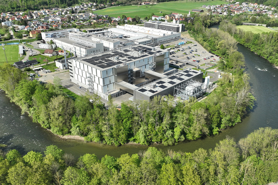
On June 3, the Austrian microelectronics manufacturer AT&S officially opened its new competence center for research and development (R&D) and production of IC substrates - printed circuit boards that can accommodate and embed a microchip - in Leoben.
After three years of construction and investments of more than € 500 million, 420 new employees are already working at the AT&S headquarters in Leoben Hinterberg in the state-of-the-art building complex 'Hinterberg 3' (HTB3). In addition to the IC substrate production sites in Malaysia and China, the completion of HTB3 completes AT&S's global research and production triangle for advanced IC substrates, which are crucial for the development and manufacture of high-performance microchips. With HTB3, Europe now has its own capacities for researching and producing IC substrates for the first time.
The new R&D center in Leoben will make the entire European microelectronics industry stronger and less dependent. It also lays the foundation for the digital and sustainable industries of tomorrow.
The new AT&S plant was funded as part of the IPCEI program, which aims to accelerate European research in the field of microelectronics. The first substrate samples have already been delivered to some customers, and qualification for new products is proceeding according to plan.
