This year, PCB manufacturer KSG has invested around 11.6 million euros in its two plants in Gornsdorf and Gars am Kamp. In addition to expanding its production capacities, KSG is also expanding its process technology for high-speed RF and HDI/SBU PCBs.
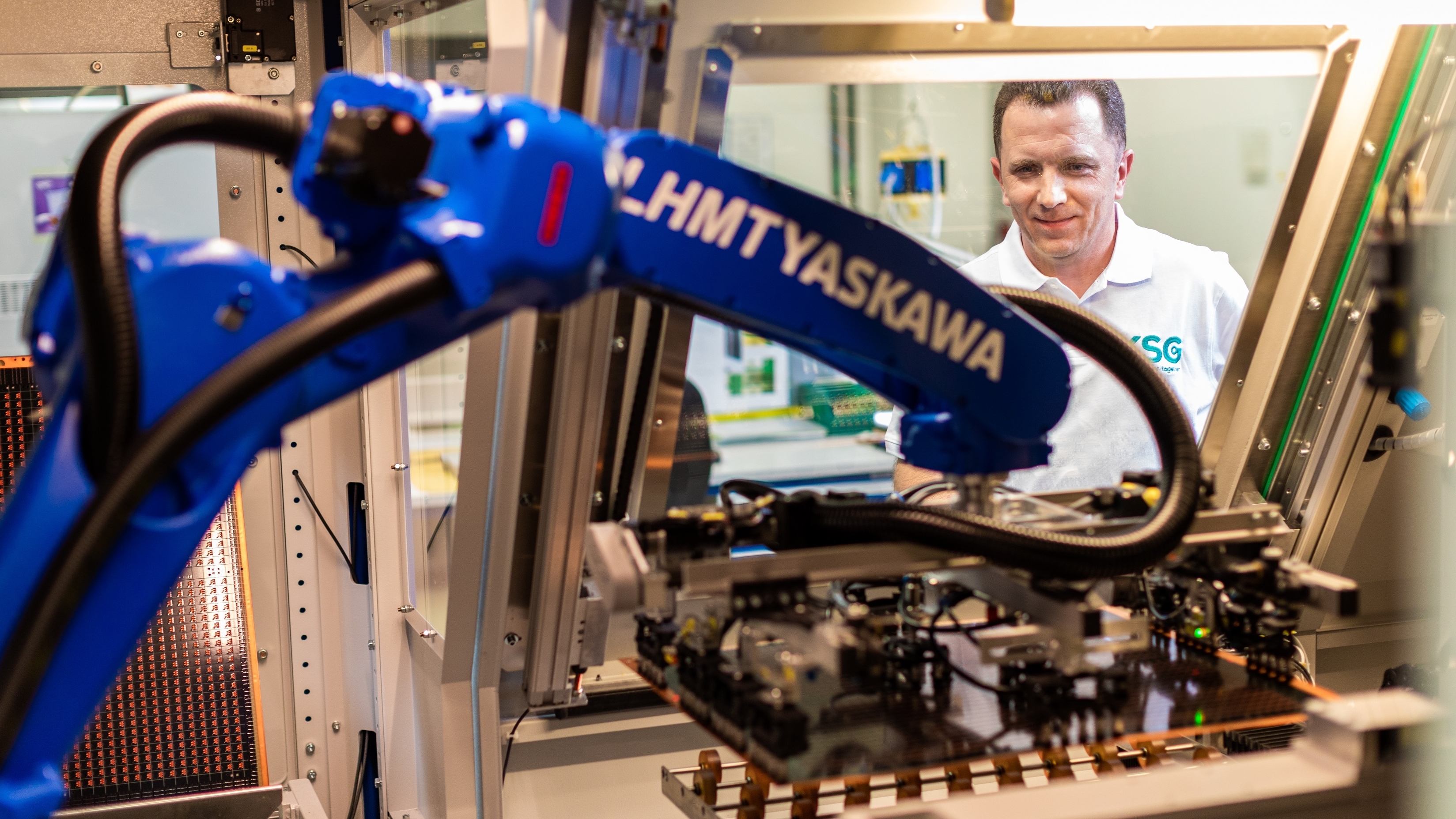
") Swen Klöden, CTO at KSG (Image: KSG)"With this year's investments, we are increasing our expertise in HDI/SBU printed circuit boards (high density interconnection/sequential built up) and continuing our course for security of supply, high product quality and flexibility," says Swen Klöden, CTO at KSG. KSG has invested around 10.8 million euros in the Gornsdorf plant in Saxony and further expanded production capacity at the Gars am Kamp plant in Lower Austria with around 800,000 euros.
Swen Klöden, CTO at KSG (Image: KSG)"With this year's investments, we are increasing our expertise in HDI/SBU printed circuit boards (high density interconnection/sequential built up) and continuing our course for security of supply, high product quality and flexibility," says Swen Klöden, CTO at KSG. KSG has invested around 10.8 million euros in the Gornsdorf plant in Saxony and further expanded production capacity at the Gars am Kamp plant in Lower Austria with around 800,000 euros.
With extensive, demand-oriented investments totaling 35.3 million euros, KSG has already converted its two sites into high-end production facilities and expanded production capacity at the Gars plant over the past three years. This year, the largest investment projects are aimed at expanding technological possibilities, increasing capacity and improving process reliability in key processes. These include the installation of the plugging process for filling drill holes and blind holes, an additional laser drilling machine and the installation of a measuring machine for measuring the conductor runs of highly complex antenna structures.
The process experts in Gornsdorf have also planned an SES system (stripping/etching/stripping), a copper recycling system and an electroplating system, which will be installed in 2021. This will provide security of supply coupled with technological expansion for the reliable production of highly complex HDI/SBU assemblies. The higher integration densities possible with this process offer PCB designers considerable space savings and fewer restrictions in the layout of complex circuits.
"Semiconductors continue to drive the development of PCB technology. For us, this means that we must continue to perfect the properties of PCBs with ever smaller dimensions," emphasizes Klöden. Today, twelve-layer HDI multilayers with a line/space of 100 µm and smaller are state of the art in Europe.
However, optimized signal integrity requires an even higher integration density. To achieve this, PCB designers are forced to combine impedance-controlled multilayers with layer structures greater than twelve layers with complex SBU structures 3+x+3 and ultra-fine conductor patterns smaller than 75/75 µm line/space. When routing fine-pitch BGA structures with several hundred connections on the underside, rewiring strategies with plugged, staggered or stacked microvia arrangements are becoming increasingly important.
