Printed electronics (part 1 of this two-part article) is developing faster and in a more differentiated way than some market analysts predict. It is increasingly becoming a serious competitor to traditional PCB technology for many product types. In addition to the economy, the growing environmental problem will force the electronics industry and its customers to produce even more efficiently and environmentally friendly than before in the coming years. As a result, printed electronics are expected to establish themselves on the global market much faster and more extensively than before. Market assessments and forecasts for printed electronics show that hardly any market research company can be trusted.
Long before the 'etched film method', it was already possible to produce printed circuit boards using screen printing and/or spraying on conductive silver-based inks. The inkjet process is now well established. Since around 2000, screen printing, spray-on and/or inkjet have been combined and referred to as printed electronics (PE). Modern PE is based on the combination of new materials and large-area, high-volume deposition and patterning techniques.
Over the past two decades, thousands of articles have been published on PE. Some proponents of this manufacturing method predicted that it would replace all existing PCB technologies - on the grounds that it was environmentally friendly, both investment costs and manufacturing costs were low, etc.
PE market data difficult to determine
So far, the opposite has happened: PCB production based on conventional technologies continues to grow. One important reason for this is that the complexity and intricacy of PCBs is constantly increasing and has not yet been matched by PE.
The author has observed the development of printed electronics in the past with casual interest. He wondered what the difference is between PE and Flexible Printed Circuits (FPC). Much of PE is based on flexible materials. A considerable number of FPC manufacturers promote printing processes with conductive ink, mainly using silver particles. There must be some overlap between PE and FPC. However, in terms of electrical performance, FPC is superior to PE.
Many market studies have been published on the expected sales growth of PE. The market sizes stated or forecast by them vary widely and it is very difficult for the author to determine a 'true' PE market size. Determining the market size for printed circuit boards, on the other hand, is relatively easy for him as he has built up a huge database over the last 30 years. Nevertheless, the first part of this article will attempt to paint a picture of PE.
The second part of this article, which will be published in PLUS 3/2021, deals with 3D MID (Molded Interconnect Device; some refer 'M' to 'Mechatronic' instead of 'Molded'). The author is somewhat more familiar with 3D MID than PE, although its market size is also difficult to understand.
There are no good statistics on the number of manufacturers of PE and 3D-MIDs (material and equipment suppliers excluded). The wildest guess for PE is between 300 and 500 companies. Based on the membership lists of the European and Japanese 3D-MID associations, the number here is around 50. 99 members are listed in Europe, of which 35 to 40 are 3D-MID manufacturers, in Japan there are only 11, including 4 manufacturers of 3D-MIDs, the rest are material, equipment and design service providers.
design service providers. This is where the estimate of around 50 companies comes from - in contrast to PE manufacturers, where there are only rather nebulous ideas. However, as you can see later in this article, despite this situation, the number of companies involved in PE will grow massively over the next ten years. This will happen to the same extent that PE will gain in importance.
In view of these uncertainties, it can be interesting to compare how the global number of PCB manufacturers has developed over the last two decades in comparison to the producers of PE and 3D-MID.
PCB producers by world region
The author has been tracking the number of PCB manufacturers around the world for many years. Towards the end of the 1990s, foreign manufacturers began to invest in China. Investment there accelerated from 2000 onwards, as shown in Table 1. And conversely, the number of manufacturers in North America, Europe and Japan declined. Nobody, not even the Russians themselves, knows the exact number of PCB manufacturers in Russia. If you ask ten people, you will get ten answers. Nevertheless, the figures in Table 1 probably reflect the real situation. In Table 2, the author estimates the number of board manufacturers for 2019 to the best of his knowledge.
Table 1: Historical development of the number of PCB companies worldwide from 2000 to 2010 by region or country
|
Country/Region |
2000 |
2001 |
2002 |
2003 |
2004 |
2005 |
2006 |
2007 |
2008 |
2009 |
2010 |
|
China |
650 |
720 |
780 |
830 |
870 |
900 |
930 |
980 |
1020 |
1100 |
1150 |
|
North America |
780 |
745 |
680 |
560 |
520 |
488 |
460 |
427 |
353 |
340 |
325 |
|
Japan |
380 |
360 |
350 |
345 |
330 |
320 |
310 |
290 |
285 |
280 |
280 |
|
Europe |
690 |
625 |
530 |
478 |
426 |
379 |
342 |
319 |
307 |
256 |
230 |
|
India |
100 |
100 |
105 |
107 |
110 |
110 |
115 |
118 |
120 |
122 |
125 |
|
Taiwan |
130 |
130 |
127 |
120 |
115 |
110 |
110 |
105 |
105 |
103 |
100 |
|
South Korea |
100 |
100 |
100 |
96 |
95 |
90 |
90 |
90 |
85 |
80 |
80 |
|
Russia |
300 |
280 |
250 |
200 |
150 |
100 |
95 |
90 |
87 |
75 |
70 |
|
South America |
80 |
75 |
73 |
70 |
65 |
60 |
58 |
55 |
51 |
50 |
45 |
|
other |
80 |
85 |
90 |
95 |
100 |
105 |
110 |
120 |
130 |
150 |
160 |
|
World total |
3290 |
3220 |
3085 |
2901 |
2781 |
2662 |
2620 |
2594 |
2543 |
2556 |
2565 |
N. T. Information Ltd
Table 2: Global number of PCB companies and production facilities by region and country for 2019 (estimate as at March 2019)
|
Type |
Type China |
North America |
Europe |
Japan |
Taiwan |
South Korea |
S. E.A.* |
India |
South America |
ROW** |
World |
|
Number of |
1200 |
220 |
202 |
160 |
80 |
70 |
80 |
130 |
37 |
130 |
2309 |
|
Number of |
1600 |
240 |
220 |
190 |
120 |
90 |
90 |
130 |
37 |
130 |
2847 |
*S. E. A.: South East Asia(N. T. Information Ltd)
** ROW (Rest of the World), incl. Africa, Middle East, Russia (rough estimate)
Interesting conclusions can be drawn from the comparison of the two tables. Examples:
- The cumulative number of board manufacturers in the world decreased steadily on average from 2000 to 2019(Tables 1 and 2) The number of manufacturers, still around 2309 in 2019, would be even lower if China had not bucked the continuous downward trend with many new start-ups
- The number of Chinese PCB companies almost doubled between 2000 and 2010, but has not grown dramatically since then. However, the number of plants per company has increased
- The number of PCB companies in North America and Europe roughly fell to around a third each between 2000 and 2019
- The number of PCB manufacturers in Russia fell by around a fifth between 2000 and 2019 (approx. 60 companies in 2019) PCBs are sourced from China, Taiwan or South Korea - depending on the level of difficulty, and some are already assembled
- The number of board manufacturers in South America has more than halved between 2000 and 2019 and now stands at 37, compared to almost half the number of PCB manufacturers in Germany
The figures change every month worldwide, for example due to the recent insolvencies in Germany (Straschu, Schoeller Electronics Systems). Taiwan offers some examples of the great market dynamics: Dynamic of Taiwan closed its production in Taiwan in 2019. In October, Mutual-Tek Industries Co. announced that the plant in Taiwan would be closed due to the losses caused by Huawei (a consequence of Trump's sanctions). Around 600 employees will be made redundant. Mutual-Tek is now moving production from Taiwan to its Chinese plant in Jiangsu. However, Taiwanese board manufacturers Flexium Interconnects and ZDT are building new facilities in Kaoshiung (Taiwan), presumably for LCP antennas.
In China, there are a number of manufacturers that are merging and building new production facilities despite complaints about overcapacity and uncertainties about the future market. For large growing manufacturers, new investment does not seem to be a death sentence. It is impossible to make a useful forecast for PCB production in 2021, but it will definitely continue to grow in the future. Printed electronics is facing a similar situation. The trade war between the US and China is not slowing down China's PCB dominance (including Taiwan's share in China).
In any case, it can be assumed that, in contrast to the stagnating number of companies in the PCB industry from a global perspective, the number of companies in the PE sector will rise sharply in the coming years, as PE is still at the beginning of its future curve. This is demonstrated by the following statements. Another fact is that PE is increasingly 'grazing' parts of the PCB industry's production spectrum with its own solutions. This has consequences for the PCB industry.
Printed electronics
Printed electronics is based on the combination of new materials and large-area or digital selective deposition and structuring techniques with high volumes. A number of printing processes enable the printing of electronic and photonic components using conductive or semi-conductive inks and various substrates (mainly plastics and fabrics). Such processes can include screen printing, flexography, gravure printing, offset lithography and inkjet. These techniques can be used to produce printed resistors, capacitors, transistors and many other electronic components.
 Fig. 1: Demonstrator of the AM-OLED with 62,967 pixelsPrintedelectronics are considered to be simple, inexpensive and time-saving to produce. The processes are very environmentally friendly. Although the performance of the products is still relatively low in comparison to traditional PCB technology, they are now moving into more complicated and complex areas. Examples of this are OLED displays. The carrier materials for PE are usually very thin, light and flexible and can be integrated into existing production lines for printed products. These advantages are proving attractive for many existing applications and are inspiring new applications.
PE is a rapidly growing field that opens up new possibilities, such as intelligent containers, packaging, artistic designs with a dual function as lighting fixtures, flexible screens and much more. New applications are constantly becoming possible in the consumer electronics, packaging, printing, automotive, medical and pharmaceutical industries, among others. Market analysts try to record the status and further development of PE technologies and products and map them in forecasts.
There are a number of market research companies worldwide that deal with PE. However, they come to very different conclusions about how the market will develop over the next few years. This has to do with how printed electronics is defined as a product group, i.e. what is included in it.
Some market research companies roughly divide the applications into these five main clusters:
- OLED lighting
- OLED displays (mostly flexible)
- Printable organic photovoltaics (OPV)
- Components and modules (printed storage and batteries, active and passive components)
- Integrated intelligent systems and objects (RFID, sensors and intelligent textiles)
It should be noted that OLED technologies are often assumed to be part of PE. This is a misunderstanding (www.oled-info.com/), as almost all OLED panels are currently not produced using printing technologies, but rather using traditional vapor evaporation. Although research work has been underway for many years to produce not only small displays for display panels, for example, but also large-area displays using a combination of different printing techniques, achieving 8K resolutions, for example, is a distant goal.
One example of such a research project in the OLED sector is the EU-funded Hi-Response project, which ran until 2019. In addition to the Fraunhofer Institute for Applied Polymer Research IAP, 12 other partners were also involved. Together with the project partners imec and TNO/Holst Centre, the IAP developed the high-resolution ESJET process, a pulsating electrostatic jetting process with electrically conductive and light-emitting polymers for the production of AM OLEDs. It was possible to realize displays with 62 967 pixels with a pixel resolution of 10 µm(Fig. 1). The process, which is classified as printed electronics, is scalable and particularly interesting for larger OLED display formats. However, work still needs to be done on this. The Japanese company Joled Inc. has already made significant progress with PE displays.
Due to this incorrect classification of conventional OLED technologies as PE by some market research companies, the market for this type of product is often definitely overestimated (inflated). For example, there is sometimes talk of annual sales of $20 billion or more. However, around $15 billion of this is accounted for by sales of OLED panels, even though the vast majority of these OLEDs do not use any printing processes at all. A relatively small remainder could then really be PE. At least that was the situation until 2019, and this remainder does not even appear in the PE group in the forecasts. This issue of classifying OLEDs in market analyses will come up again in a moment and makes it difficult to produce true trend analyses.
The market for PE at IDTechEx
By far the most important market and trend analyst for PE is the US company IDTechEx Research, Boston, founded in 1999. The website www.idtechex.com states that the company employs around 200 people. It organizes conferences on printed electronics worldwide. PE news has been flowing continuously from the company to the world since around 2002. It has published many articles on the subject, including regular market assessments.
In 2011, IDTechEx Research published the market study 'Printed, Organic & Flexible Electronics Forecasts, Players & Opportunities 2011-2021', which included Figures 2 and 3. This study was chosen in order to have comparisons with the current situation and to be able to better assess the speed of PE's forward development.
What do these three terms in the title mean?
- Printed electronics: functional electronics produced by creating conductive traces and insulating layers using one of several printing methods, e.g. screen, inkjet, gravure, flexographic and others (not to be confused with traditional printed circuit boards)
- Organic electronics: Production of circuits made of conductive polymers or smaller organic compounds on carrier materials made of organic films and with conductor tracks and components made of conductive organic molecules (organic semiconductors). Synonyms: plastic electronics, plastic electronics or polymer electronics
- Flexible electronics: A class of electronic products built on customizable or stretchable substrates, usually plastic, but also metal foil, paper and flex glass (not to be confused with flexible printed circuit boards)
The terms organic electronics, polymer electronics or flexible electronics are often used as synonyms for printed electronics due to the obvious similarities. This close interdependence of the three terms mentioned above is one of the main reasons why IDTechEx treats printed, organic and flexible electronics together in one study and jointly considers their products. The combination is obvious.
IDTechEx has also included OLEDs, OLED lighting and photovoltaics in its PE market study. One reason for this may be that all three can increasingly be produced using printed electronics methods. The "shift" in the production of OLEDs and photovoltaics towards PE, which is slowly gaining momentum, will have a significant impact on the size of the PE market volume in the future. The challenge for market researchers is to find out how quickly and intensively this shift is taking place, i.e. how much of the production of these three product groups can be attributed to "real" PE, which is the focus of this article.
The same can be said about sensors. More and more classic sensors are being manufactured on flexible films and are therefore moving over to PE. For example, the Danish company Mekoprint A/S commissioned a new, highly productive special printing line in November 2020, which can be used to screen print stretchable electrical circuits on films using the roll-to-roll process for healthcare applications - up to 20 km per day. Wearables for healthcare applications are a rapidly growing segment for PE.
OLED lighting can now also be produced using soluble materials and printing technologies. Two Japanese companies in particular are currently producing such OLEDs: Konica Minolta and Pioneer/Mitsubishi. The exact production methods of these companies are not known. Konica Minolta recently began mass producing 'Lighting Paper'. This is a new printing solution where paper-thin, lightweight and flexible OLED lighting panels are applied to product packaging, advertising and greeting cards.
Printed electronics still 'small' in 2011
In Figure 2 of its 2011 market study, IDTechEx summarized the product groups OLEDs and photovoltaics as 'Not Printed' and classic PE products as 'Mostly Printed'. It should not be forgotten that this was the situation in 2011, and therefore also the state of the OLED industry at that time.
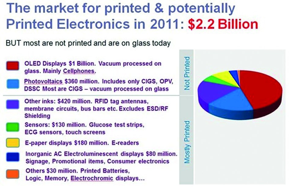 Fig. 2: Breakdown of total sales of the market for 'Printed' and 'Not Printed Electronics' into the individual application areas in 2011 with sales of $2.2 million. Image: IDTechEX
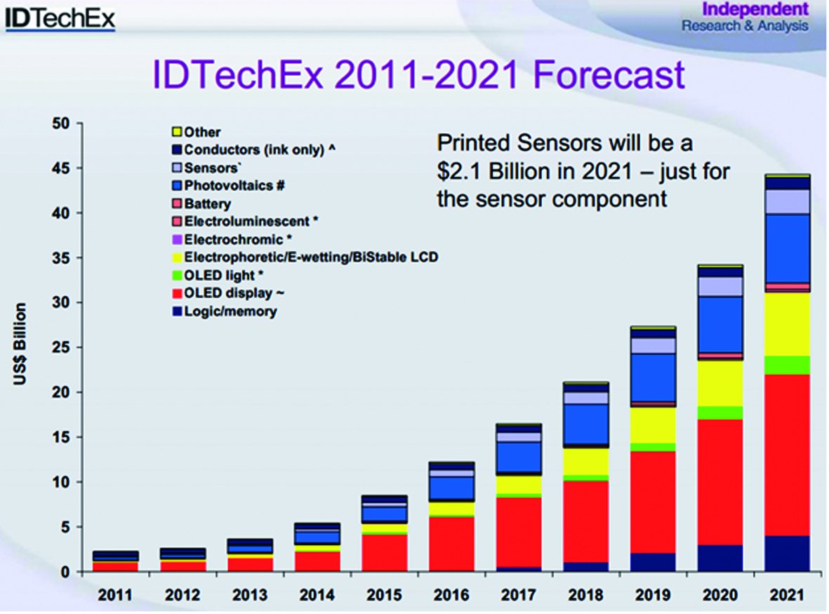 Fig. 3: Forecast of the development of revenues for 'Printed' and 'Not Printed Electronics' from 2011 to 2021, broken down by product type. Image: IDTechEX
The illustrations in Figures 2 and 3 are organized by product type. The predictions in the PE section include both planar (rigid and flexible) and spatial carriers (3D printing). This is because the classic methods of printed electronics for the realization of electrical components and electrical circuits can be applied to both types of carrier(Fig. 4).
According to Figure 2, total global sales of the two product areas 'Mostly Printed' and 'Not Printed' amounted to around 2.2 billion dollars in 2011. The classic product area of PE accounts for 38% of this total, i.e. $836 million. The chart also shows that printed electronics already included a very large number of applications at that time, ranging all the way to printed batteries, logic and memory circuits. However, OLED displays are not yet included here.
IDTechEx has set itself the task of showing how the overall market in both areas is developing in the annual updates of this study. More and more products should actually be moving from the 'Not Printed' to the 'Mostly Printed' sector, because the increasingly massive environmental demands are also putting more and more pressure on the industry to manufacture in a more environmentally friendly way and are also driving technical progress. However, this is not yet evident at IDTechEx.
In Figure 3, the market researchers at IDTechEx ventured a prediction for the development of sales of the two product areas in Figure 2 of the study by product type up to 2021 from the perspective of 2011. According to estimates at the time, sales could then total USD 45 billion. The market researchers assume exponential development. Assuming that traditional PE grows with a share of 38%, as stated at the beginning of Figure 2, turnover in 2021 would be in the region of USD 29 billion. However, this is far from the case, as we will see in a moment. According to the NTI 100 list, the $29 billion would correspond to around 40% of global PCB production in 2019 (approx. $62 billion). But this is all speculation.
Printed electronics is growing steadily
In October 2018, IDTechEx published an update of its study 'Flexible, Printed and Organic Electronics 2019-2029'. It states that the total market for printed, flexible and organic electronics and OLED displays amounted to USD 31.6 billion in 2018(Fig. 5). This is 14 times the total amount of $2.2 billion stated in the 2011 study. It is significantly more than the 2011 forecast of around USD 20 billion for 2018 in Figure 2.
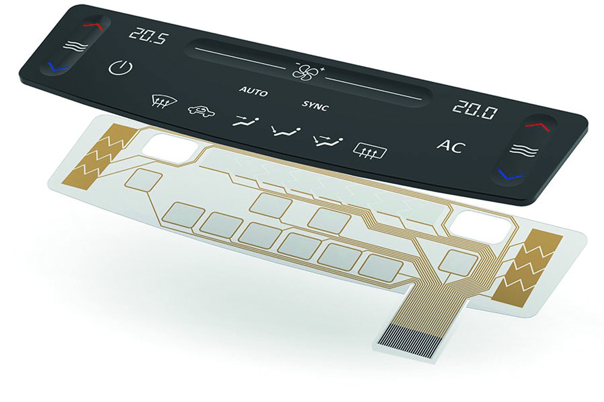 Fig. 4: Examples of printed electronics :
 planar (left) and 3D circuits (right)
Conclusion: The development of the market as a whole is much faster than IDTechEx assumed in 2011. However, displays are primarily responsible for this enormous increase with a share of USD 26 billion, primarily OLED displays. The latter have only experienced a rapid upswing in the eight years since 2011. Other display types such as electrophoretic displays, which are used in e-readers and for electronic shelf labels, only account for a small share.
However, the classic printed electronics sector, the other four product areas on the right in Figure 5, also made a measurable contribution to the increase to USD 31.6 billion in 2018 with USD 5.57 billion. It could be higher if IDTechEx had already included the product group PE-OLED lights for cars. As it is, the share is only around 18% - in contrast to 38% in 2011. Although the growth of conventional PE is therefore much slower than that of displays, it is still very much on target. While the total sum of the two product areas examined in the study, 'Not Printed' and 'Mostly Printed', increased fourteen-fold between 2011 and 2018, this figure is only seven-fold for conventional PE.
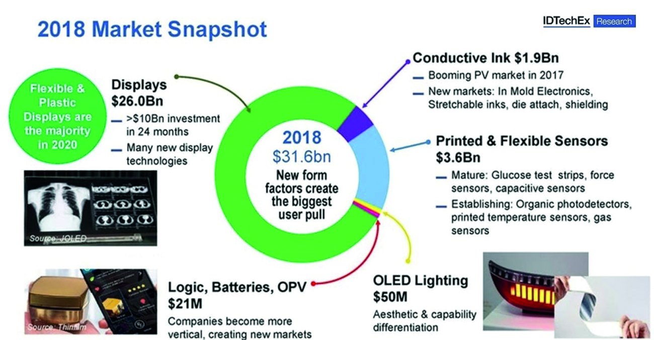 Fig. 5: Current market status of Printed and Not Printed Electronics for 2018 in the IDTechEx study for 2019-2029. image: IDTechEX
According to IDTechEx, the sum of classic PE is expected to rise to $8.5 billion in 2029, which can perhaps be assumed to be an oversight due to the 11-year difference to 2018. This figure is most likely far too low and therefore incorrect, as the analysts have not taken into account the fact that printed electronics is poised to make massive inroads into the automotive industry, sensor technology and medical technology, for example, over the next decade, i.e. 2021 to 2030.
In January 2020, IDTechEx consequently corrected the figure: the market researchers are now predicting growth to $20 billion for 2029. However, even this figure is probably far too low and will require a further significant correction in the upcoming market study for 2021 to 2031.
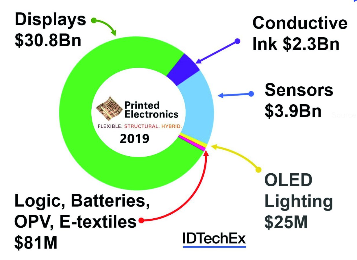 Fig. 6: Current market status of printed electronics for 2019 in the IDTechEx study for 2020-2029Inthe PE sector, OLED lighting is already represented in 2018, albeit with a low figure of USD 50 million. In 2018, the authors of the study were of the opinion that flexible and plastic displays would already outweigh rigid glass-based displays in 2020 - but in what type of production? Even the displays of the folding smartphones now appearing on the market are still manufactured in the traditional way in Japan and South Korea.
Figure 5 is an excerpt from the IDTechEx market study 'Printed, Organic & Flexible Electronics Forecasts, Players & Opportunities 2020-2030', which was published in 2019. According to the market analysts' estimates, the total market for the five product areas in Figure 5 grew from $31.6 billion in 2018 to $37.1 billion in 2019, i.e. by 17%, in just one year. This sum is also much higher than assumed in the 2011-2021 study at around USD 27 billion for 2019(Fig. 3). It is a prime example of how market research companies are overwhelmed by reality when preparing relatively long-term forecasts - even if this mainly affects the displays product group.
Classic printed electronics, again the other four product areas on the right in Figure 6, has a share of USD 6.3 billion. The increase from 2018 to 2019 is 13%. The figure shows that the product groups conductive inks, printed and flexible sensors as well as logic circuits, batteries, OPV and e-textiles increased significantly in 2019 compared to 2018. It will be interesting to see the follow-up study for the period 2021-2031, but IDTechEx is having problems with this due to coronavirus.
Other market analysts
Sometimes it is interesting to look at the forecasts of other market research companies. For example, the following analytics companies have also published analyses on printed electronics:
- P&S Intelligence, India (period 2019 to 2030)
- Coherent Market Insights, India (2018-2025)
- Million Insights, India (time span 2014-2025)
- Research and Markets, Ireland (time span 2020-2025)
- Grand View Research, USA (time span 2018-2025)
- Envision Intelligence, USA, India (time span 2020-2026)
- Markets and Markets, USA (time span 2020-2025)
- Zion Market Research, India (time span 2020-2026)
This list is not exhaustive for reasons of space. The studies often deal with global trends, sometimes only with specific regions of the world. The figures published by the companies mentioned sometimes differ considerably from each other and also from the values determined by IDTechEx, because the approaches are often different. Examples:
The Indian company Prescient & Strategic Intelligence Private Limited, based in New Delhi (also known as P&S Intelligence), is ahead of IDTechEx with its market values. In 2019, the company published the study 'Global Industry Trends Analysis and Growth Forecast to 2030' on printed electronics. It also includes displays in the form of electroluminescent and electronic paper (e-paper) versions. The global market for printed electronics is estimated to be worth USD 35.7 billion in 2019. This is around five times more than IDTechEx. For 2030, the Indians expect the market to grow to an estimated $363.1 billion.
 Fig. 7: 4k OLED display, manufactured with the new JOLED technology
 Fig. 8: Development goals for the future of Joled Inc.
This figure is unbelievable at first glance, but not impossible from the author's point of view. It corresponds to a CAGR of 22.4% during the forecast period 2020-2030. According to the study, the PE market is expected to show the fastest growth in the Asia-Pacific (APAC) region during this period. The market researchers assume that a large proportion of classic OLED displays will already be realized using PE-based methods by 2030 in order to meet the demand for material and weight reduction, flexibility and environmental friendliness. According to the authors, flexible ICs on flexible substrates will be a basic component of printed electronics by then.
In its 2020-2025 market study, the Irish company Research and Markets estimates the value of PE in 2019 very accurately at $15.338 billion (how does that work?) and sees annual growth (CAGR) of 16.83% until 2025. The figure for 2019 is double that of IDTechEx.
The Indian analytics firm Coherent Market Insights estimates in its 2017 study 'Printed Electronics Market 2018-2025' that the market value of PE will reach around $22.3 billion in 2025. While IDTechEx predicts $20 billion for 2030, the Indian market observers assume a similar sum for 2025.
Printed electronics set to soar
If more and more OLED displays are manufactured using inkjet printing based on the new JOLED technology in the future, the PE sector could receive a significant boost in the coming years. It could take a significant share away from classic OLED displays, which have largely been assigned to the not-printed sector at IDTechEx to date. In November 2019, the Japanese company Joled Inc. began manufacturing small and medium-sized OLED displays using PE methods in Nomi.
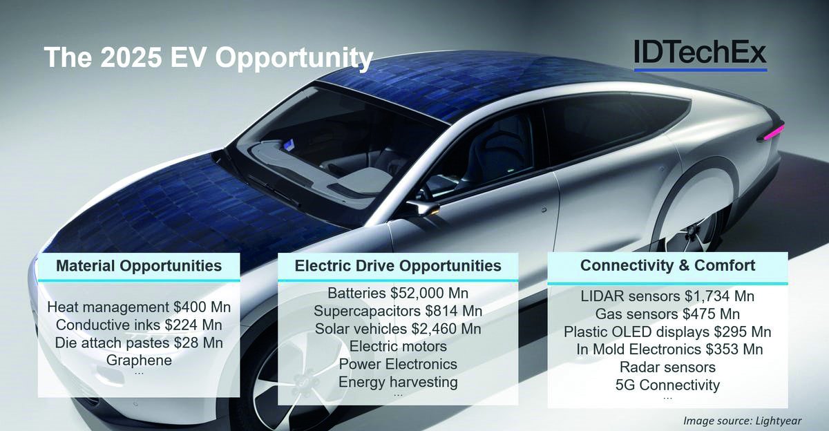 Fig. 9: Electric cars offer many possible applications for PE
For example, the 21.6 inch 4k OLED displays are only 1.3 mm thick and weigh just 500 g (without frame and stand)(Fig. 7). The screens range from 10 to 32 inches (80 cm diagonal). The company is continuing its research into the production of even larger and foldable displays for the consumer sector(Fig. 8). The new displays will initially be used in monitors for medical and professional purposes from 2020.
According to the latest reports, the displays will also be used in aircraft cabins, e.g. at Lufthansa, and also in the automotive industry. The first practical applications are currently underway in the train station stores of the Japanese JR East Retail Net Co., Ltd. IDTechEx will probably have to set up a new product group for the new OLEDs in its PE study for 2021 in the 'Not Printed' area in order to be up to date.
The transition to electric cars offers many opportunities for printed electronics. Vehicle manufacturers worldwide are currently investing in the introduction of In-Mold Electronics (IME) technology to further integrate vehicle electrics such as dashboards, control modules and control units based on PE. In-Mold Electronics is the combination of traditional In-Mold Decorating (IMD) technology with printed electronics. Today, Tesla and Ford are already using silver nanoparticle materials and graphene for IME. It is seen as a revolutionary new way of integrating electronics into plastics, which the Japanese company Nissha, together with its US subsidiary GSI, is particularly committed to.
 Fig. 10: Symbolic graphic of the Japanese company Nissha showing how IME is changing the technology processes for automobiles
It is a modular product in which functional parts such as touch sensors, light sources, heaters and antennas are integrated in plastic. IDTechEx has provided examples of the use of PE solutions in electric cars in 2025 and the expected sales in Figure 9. Some of them will be realized in IME technology. In Figure 10, Nissha provides symbolic information on how IME will change existing work processes. They will become more efficient. Figure 11 contains suggestions for the use of IME in the automotive cockpit as well as information on the improvements that can be achieved. They come from the Californian company Namics. Figure 12 shows an example of a dashboard display module manufactured with IME from Nissha/GSI.
Unfortunately, the rapidly growing sales of PE in the automotive sector will probably be partly at the expense of the traditional PCB industry. Not so long ago, for example, the industry began to replace conventional wiring harnesses with long flex boards.
Namics' novel stretchable inks and pastes offer designers and engineers the freedom to develop next-generation in-mold electronics (IME) that combine in-mold decoration processes with electronic inks. The result is interesting functional parts for automotive, medical, industrial and consumer electronics.
Other examples of new up-and-coming PE applications that will have a massive impact on production figures include flexible rollable OLED displays, Covid-19 test strips, smart home electronics, RFID tags for smart packaging, IR sensor elements and more.
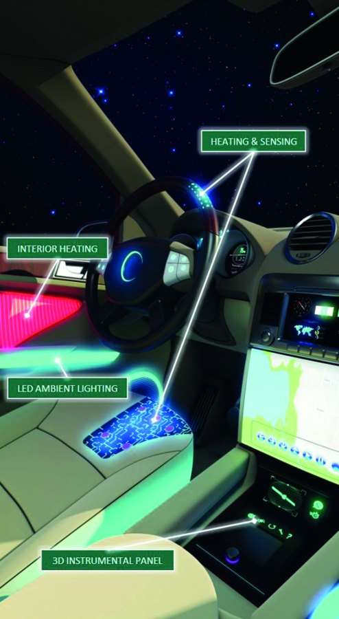 Fig. 11: Application examples of IME technology in vehicles from Namics
 Fig. 12: Integrated display module for the dashboard, manufactured on the basis of IME by Nissha/GSI (right)
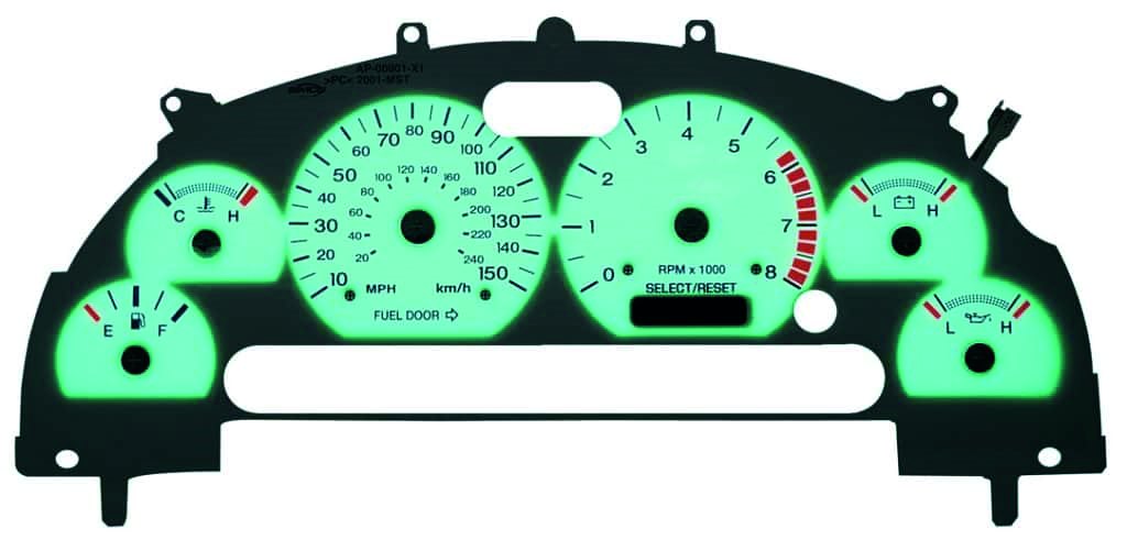
US-based Drexel University has introduced a range of ultra-thin, flexible, spray-produced 5G antennas that are a fraction of the weight and thickness of conventional copper antennas(Fig. 13). The coating can be applied by screen or inkjet printing on almost any type of substrate and remains flexible without sacrificing performance.
The researchers found that titanium carbide MXene can be dissolved in water to create an ink or paint that exhibits exceptional conductivity. The MXene antennas with layer thicknesses around 8 µm were 50 times better than graphene and 300 times better than silver ink antennas in terms of maintaining the quality of radio wave transmission.
The process could open the door to new applications in smart technology, wearables and IoT devices.
European companies are also making an important contribution to the development of printed electronics. The Danish company Mekoprint announced at the beginning of December 2020 that it had started mass production of sensors based on new carrier materials. It sees an increased demand for such sensors, which can also be stretched while retaining their electrical conductivity. The sensors are applied to a paper-thin nonwoven using a roll-to-roll process and screen printing.
 Fig. 13: MXene 5G antenna produced by Drexel University using the PE processThenonwoven material can be stretched, shrunk, folded and torn. "This type of printed sensor will be an essential part of an IoT future. In addition, our strategic focus early on was to succeed with production at a level that allows us to keep pace with our customers' development," said CEO Morten Christensen(Fig. 14, 15). Mekoprint offers a whole range of PE solutions in high-volume printing electronics.
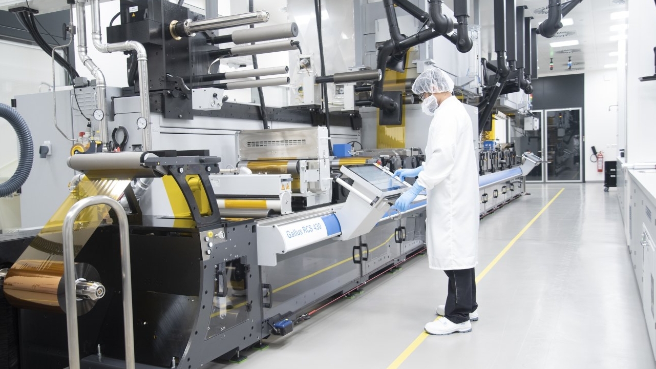
In summer 2020, Heidelberger Druckmaschinen AG launched a completely new business segment at its main plant in Wiesloch-Walldorf with the production of printed organic electronics. In the new process, a conductive ink containing sensors is printed onto a film mat instead of printing ink(Fig. 16 - title). Each square meter of the film is equipped with up to one million sensors that register the smallest changes in pressure, temperature or humidity and report them to the computer. The company invested around five million euros in setting up the production line in a clean room. "In the field of printed and organic electronics, we no longer sell the machines, but manufacture the required products ourselves," explained Heidelberg CEO Rainer Hundsdörfer.
It is produced on a further developed Gallus printing press, which was originally used for color printing of colorful images. The production facility was developed in collaboration with InnovationLab GmbH (iL), BASF SE, SAP SE, the Karlsruhe Institute of Technology (KIT) and Heidelberg University. Up to 160 serial meters per minute (~10 km/h) can be produced in continuous operation. With around 20 million 5x1 cm² units per day, an unprecedented production speed of sensors is achieved at previously unattainable low costs.
 Fig. 14: Morten Christensen (left), Director of Quality and Technology, and CEO Anders Kold (right) at the inauguration of the new production facility at Mekoprint
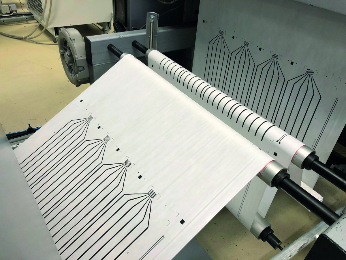 Fig. 15: Printed stretchable sensor from Mekoprint
Researchers at the Karlsruhe Institute of Technology (KIT) have developed a fully compostable display using an inkjet printing process(Fig. 17). "With our development, we were able to produce sustainable displays for the first time from predominantly natural materials using industrially relevant production methods. They do not contribute to electronic waste after use, but can be composted," says Manuel Pietsch, researcher at the Light Technology Institute (LTI) at KIT in Heidelberg. The function of the display is based on the electrochromic effect of the organic base material used. Electrochromic displays are characterized by low energy consumption and a simple component architecture compared to commercially available displays such as LEDs, LCDs and e-paper, according to the KIT. The materials used are mainly of natural origin or biocompatible. The display is suitable for short-lived applications as an indicator for sensors or simple displays in various fields, e.g. diagnostic applications in medicine, the food industry, etc.
Final thoughts
To conclude, let's make a small fictitious calculation for the automotive sector alone: in 2019, global car production amounted to 67 million vehicles. If various modules or assemblies were to be realized with IME methods in around 50 million vehicles in 2025, this would already amount to $100 billion, assuming a cumulative price of around $2000 per vehicle. From this perspective, the above-mentioned opinion of the market research company P&S Intelligence that PE could reach a market volume of over 300 billion dollars by 2030 is no longer a fantasy. The automobile is just one example of how PE will make massive inroads into new, lucrative areas of technology in the coming years. From today's perspective, there are good reasons for this.
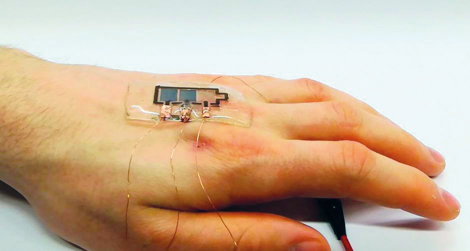 Fig. 17: Compostable display by KIT researchers
The work of market research companies, including IDTechEx, reveals a serious flaw. They are primarily trying to determine how PE sales will develop by 2025 or 2030 from a technology and market perspective. This is too one-sided, because the environmental problems, which will intensify enormously in the next 10 to 20 years, will have a profound impact on the industry that we probably cannot even foresee now.
The Paris Climate Agreement of 2005 set the goal of keeping global warming to well below two degrees, or preferably 1.5 degrees, by 2030. In view of the limited progress made so far, the European Union significantly tightened its climate target for 2030 in December 2020. Greenhouse gas emissions are to be reduced by at least 55% below the 1990 level by 2030. The previous target was minus 40%.
"In the printed and organic electronics sector, we no longer sell the machines, but manufacture the required products ourselves"
This will not be the last tightening. It is highly likely that social forces such as the Friday for Future movement will massively increase their pressure on governments and industry when they see how slowly these targets continue to be implemented. It can be assumed that the pressure on companies to switch to more environmentally friendly processes and products will take on an unprecedented intensity. Companies will have to prove that they are among the "good guys". In the electronics industry, this will lead to an increased transition to low-energy and efficient manufacturing processes such as printed electronics. A rewarding field of work for young researchers is to determine where such electronic products, which are manufactured using energy- and material-consuming, possibly even toxic processes, could be converted to PE. From this perspective, the potential of PE is still far from being fully explored.
"Sustainable displays ... They do not contribute to electronic waste after use, but can be composted"
The current situation is somewhat reminiscent of the 1990s in Japan, when the 3R movement emerged: Recycle, Reduce, Reuse. Recycling more and using less material and energy is more relevant today than ever. On October 1, 2019, the European Union issued 10 implementing regulations on the ecodesign of electrical appliances, which came into force on January 1, 2021. In future, appliances must be easier to repair and recycle and consume even less energy. Despite these directives being implemented relatively quickly, environmental associations, consumer advocates and the repair industry are not yet satisfied. From the perspective of these stricter EU resolutions, the Japanese RRR could serve as a guideline in Europe in a form adapted to the present day: RRRC: Recycle, Reduce, Repair, Change. Switch to new environmentally friendly technologies such as printed electronics.
Translation, editing and additions: Dr. Hartmut Poschmann
References:
[1] www.idtechex.com/en/research-article/printed-electronics-what-can-we-do-better/3708
[2] www.printedelectronicsnow.com/contents/view_breaking-news/2018-10-29/idtechex-identifies-printed-electronics-trends/
