Do you know the value chain of North Sea crabs before they end up on the crab roll? After being caught and cooked on the fishing boat, our crabs are flown to Morocco. There, the crabs are peeled out of their shells by hand by low-cost workers before being flown back to Germany.
Why am I telling you this? Because despite all the European chip euphoria, with the construction of chip factories subsidized with billions of euros to make Germany and Europe more independent, the other processes in the value chain are being forgotten.
The USA is thinking ahead with PCBs and substrates
The US government has proposed a $3 billion government stimulus bill to revitalize PCB production.
The bipartisan 'Protecting Circuit Boards and Substrates Act of 2023' aims to complete the activation of the US semiconductor industry along the value chain that began with the CHIPS Act. This will create incentives for investment in the domestic PCB industry.
Over the past 20 years, PCB production in the USA has shrunk from 30% to less than 5% of the global market share. Ninety percent of global supply now comes from Asia, 56% of which comes from production facilities in China alone (Fig. 1).
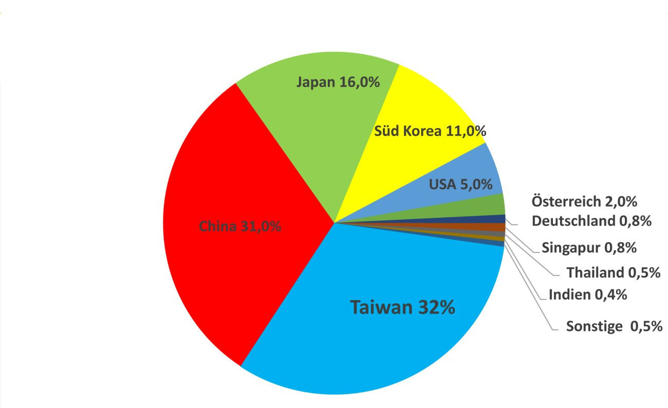 Fig. 1: PCB production worldwide in 2022 by company location
Key provisions of the bill include $3 billion to fund new PCB factory construction, skills training and research and development. There is also a 25% tax credit for buyers of American-made PCBs and substrates.
Re-industrialization instead of European de-industrialization
The 'Protecting Circuit Boards and Substrates Act' offers incentives for US companies to produce printed circuits in the country. This will also restore the supply of sensitive military electronic components and make systems for national security, such as aerospace, independent of imports. In addition to semiconductors, the US government wants to rebuild the entire microelectronics ecosystem in order to reduce dependence on China.
The semiconductor market is expected to
recover in 2024
The semiconductor market reached a new record turnover of around USD 600 billion in 2021. Growth slowed from mid-2022 onwards, so that $600 billion was also achieved for the year as a whole. For the current year, Gartner is forecasting a decline of -11.2% to USD 532 billion. Growth of 18.5% is forecast for 2024, with annual sales of USD 631 billion.
The growth rates at the start of 2023 are very inhomogeneous. While Taiwan and the USA will achieve growth of 42% and 50% respectively, China and the rest of the world will shrink by -23% and -18% respectively (Tab. 1).
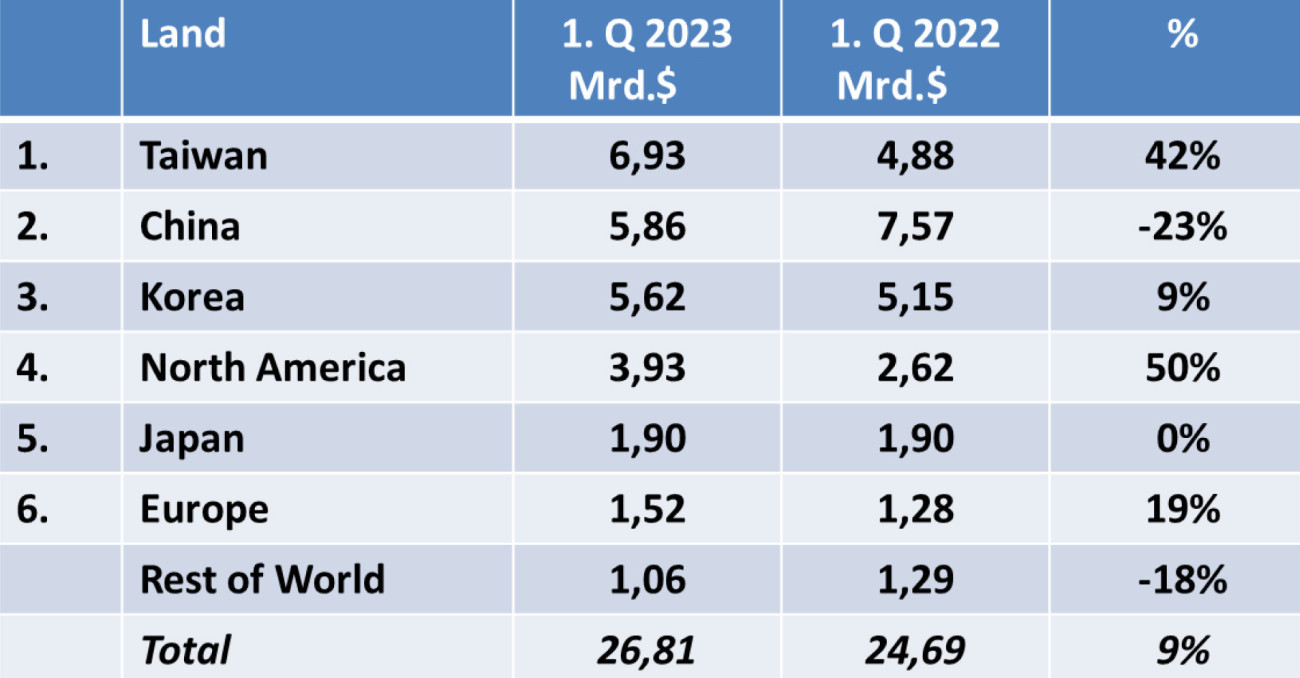 Tab. 1: Semiconductor sales by country 1st Q 2023 vs. 1st Q 2022
The market for semiconductor packaging materials is expected to grow to
29.8 billion USD by 2027
Driven by the strong demand for new electronics innovations, the global market for semiconductor packaging materials is expected to reach USD 29.8 billion by 2027 (Fig. 2). This represents a compound annual growth rate (CAGR) of 2.7% from revenues of $26.1 billion in 2022, according to SEMI , TECHCET, the Critical Materials Council and TechSearch International in their new report Global Semiconductor Packaging Materials Outlook.
High-performance computing, 5G, artificial intelligence (AI) and the introduction of heterogeneous integration technologies and system-in-package (SiP) technologies are increasing the demand for advanced packaging solutions. The development of new materials and processes that enable semiconductors with higher transistor density and greater reliability are also contributing to market growth.
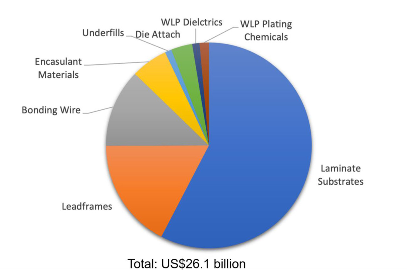 Fig. 2: Packaging material market 2022
TSMC invests in backend
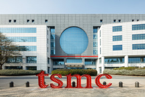 Fig. 3: TSMC Fab 6, the plant for advanced packaging and testing opened in June 2023TSMC, the world's largest chip foundry with a 54% global market share, opened the 'Advanced Backend Fab 6' in Hsinchu, Taiwan in June 2023. It is the company's first automated advanced packaging and testing fab with 3D FabricTM integration of front-end and back-end processes and testing services. The factory is prepared for mass production of SoIC (System on Integrated Chips) process technology. This involves '3DFabric Advanced Packaging' and silicon stacking technologies such as SoIC, InFO, CoWoS and advanced test processes.
Construction of the 'Advanced Backend Fab 6' began in 2020 with the aim of supporting the next generation of high performance computing (HPC), artificial intelligence, mobile applications and other products. The fab is expected to have a capacity of more than 1 million 12-inch wafers of equivalent 3D fabric process technology per year and more than 10 million hours of testing services per year.
Key technology offered will include chiplet stacking to improve chip performance and cost efficiency.
Will a chip factory for €9.9 billion in subsidies make us self-sufficient?
The contracts have been signed, the land purchased and chip production is due to start by 2027 or 2028. But despite the record subsidy of €9.9 billion, it does not yet seem clear which structure widths are to be produced here for which applications. 'Investments advance world-class semiconductor ecosystem' is the official statement from Intel.
The current state of the art is the mass production of 3 nm nodes (technology nodes) at technology leader TSMC with the plan to reduce to 2 nm (N2) from 2025.
Intel is trying to catch up and has announced its intention to produce 1.4 nm nodes in 2028.
But for Germany and Europe, this misses the point. We are neither producing high-performance computers nor the 'IPhone 15', in which the first 3 nm chips are to be installed this year. So are we subsidizing a chip factory that produces semiconductor types that are not needed in Europe?
This highly subsidized investment does not automatically mean preferential supply to German or European industry. Rather, global market conditions apply to Intel here.
However, the availability of the entire value chain from the front end to the back end will be decisive. Front-end production in the semiconductor industry is divided into three sections:
Front End of Line: in the FEOL, production begins with the bare wafer and ends with the fully assembled transistor, the heart of every microprocessor and memory chip.
Middle of Line: The MOL forms the interface between FEoL and BEoL. So-called stress layers are applied here, as well as the insulation of the transistors to the first wiring level and the contacting of the source and drain areas.
Back End of Line: The BEOL includes the metallization for the complete wiring of the circuits as well as the final passivation.
After the front end, the finished chips are contacted and the chips are separated in the back end. This also includes the testing process and final chip assembly (packaging), which is still carried out in Asia.
In a nutshell
- The US government is promoting its circuit board and substrate industry with the $3 billion 'Protecting Circuit Boards and Substrates Act of 2023'. This should provide access to all process steps along the value chain from the wafer to the packaged chip to the functional assembly in the country.
- Even though only 31% of all printed circuit boards are produced by Chinese manufacturers, the Chinese influence is much greater. Of the 32% that Taiwanese companies hold of the global PCB market by location, the majority of production is in mainland China and is therefore subject to Chinese state control at all times.
- The great efforts of the USA to build up a powerful semiconductor industry in the country and outside China can also be seen in the 50% growth in chip sales in Q1 2023 versus Q1 2022.
- TSMC has just opened Fab 6 in Hsinchu, Taiwan. This plant significantly expands the in-house capacities for advanced packaging and testing. The company is developing from a contract manufacturer (foundry) to an integrated device manufacturer (IDM) like Intel.
The entire chip value chain begins with the basic chip architecture development, which is created by ARM, for example. Fabless manufacturers such as Qualcomm, Apple and NVIDIA then develop the finished processor design. Foundries such as the global market leader Taiwan Semiconductor Manufacturing Company (TSMC) produce the chip and take over some of the testing and packaging. Then there are substrate manufacturers such as AT+S, as well as manufacturers of ABF (Anjinomoto Buildup Film) for mSAP technology and other additive and semi-additive processes! Last but not least, equipment manufacturers such as the Dutch company ASML as the market leader in EUV lithography systems ...
Which brings us to Intel's planned chip production in Magdeburg, subsidized with €9.9 billion. Perhaps it will be a lighthouse project, but it remains at best a very expensive small step towards becoming self-sufficient with chip production.
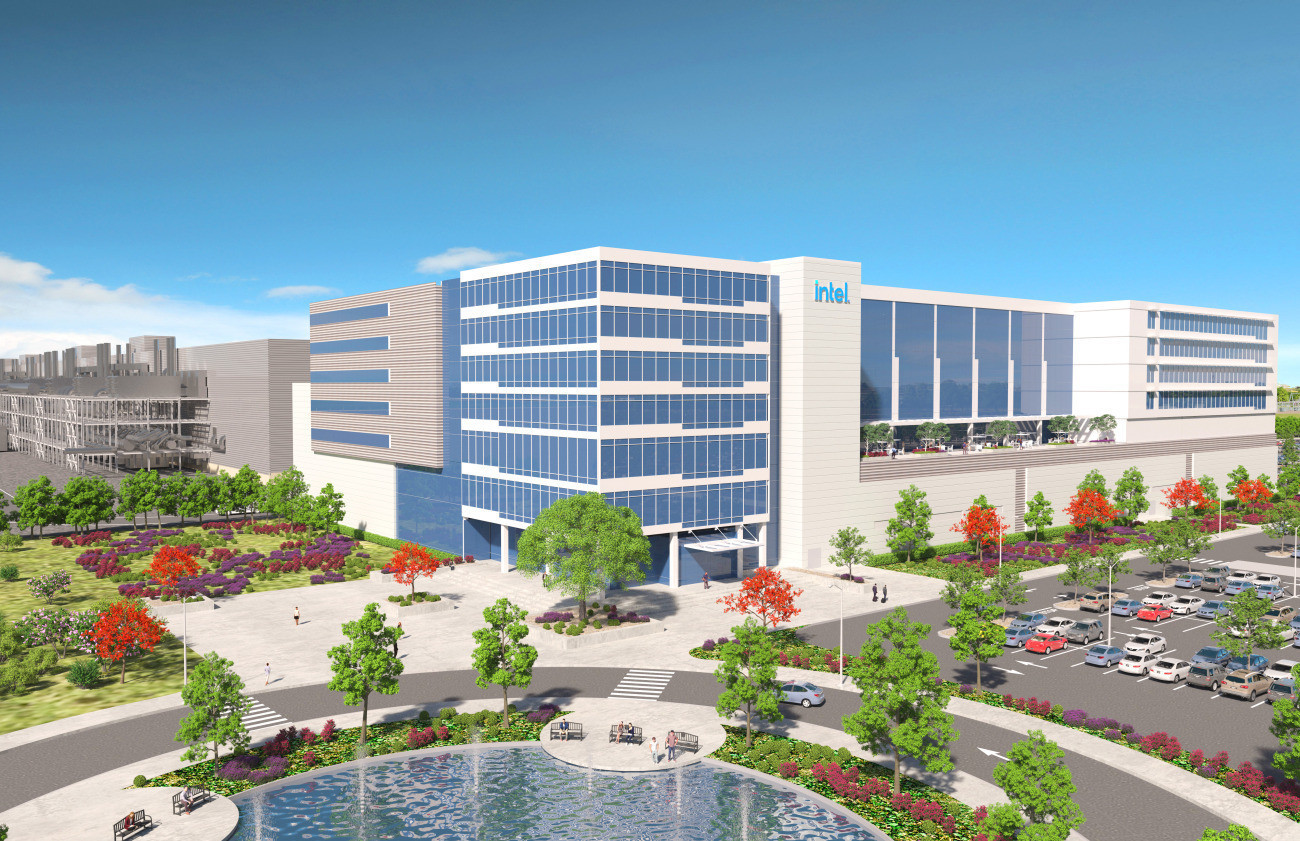 Fig. 4: Model of the Intel chip factory in Magdeburg Production ramp-up 2027/2028
Investing in German infrastructure, digitalization, education, etc. to make Germany more attractive for investment again would have made more sense.
You can't buy the future, especially not with a planned economy!
With best wishes for the summer
Yours
Hans-Joachim Friedrichkeit


