
Additive electronics manufacturing has great potential for the production of electronic or multifunctional and 3D structured components (hidronics). Printed electronics do not replace conventional circuit boards - but a new dimension in their production is achieved: Spatial circuit carriers are constructed and functionalities integrated in a single technological operation, and highly integrated three-dimensional electronic, sensitive or mechatronic 3D components are even created in a complex process module equipped with product-specific dispensing, pick & place and test and inspection adapters. And productively from a batch size of one.
 (l.) und Dr. Wolfgang Zorn (Geschäftsfeldleiter Fraunhofer-IWU) (m.)") Opening of the meeting by Prof. Reinhard Bauer (HTW and Chairman of SAET) (l.) and Dr. Wolfgang Zorn (Business Unit Director Fraunhofer-IWU) (m.)
Opening of the meeting by Prof. Reinhard Bauer (HTW and Chairman of SAET) (l.) and Dr. Wolfgang Zorn (Business Unit Director Fraunhofer-IWU) (m.)
At their first in-person meeting since the coronavirus pandemic, the members of the Saxon Working Group for Electronics Technology (SAET) learned about new findings in the field of additive technologies (Additive Manufacturing Electronics AME) for the production of multifunctional (smart) products. The event was hosted by the Dresden branch of the Fraunhofer Institute for Machine Tools and Forming Technology (IWU).
Structure-compliant integration of electrical functionalities in components
One of the technological services offered by the Fraunhofer IWU is the structured production of flat conductive and sensor structures on 3D base bodies. This enables the integration of electronics production into the conventional production of molded circuit boards, i.e. the production of conductor tracks and assembly in a single technological process. Philipp Dobeleit (IWU) explained how functionalization combines additive and conventional manufacturing. The basic technology is jet dispensing, a very robust process for the point-by-point application of electrically conductive materials for conductive structures with different properties and geometries on 3D surfaces. Thermal post-treatment using an infrared spot is used to form the conductivity, conductive path or functional element. The functional properties of the printed structures are determined by the layout, material properties and process control. The process is flexible, cost-saving, reduces the amount of purchased parts, reduces installation space and weight and is possible in places that are otherwise difficult to access. This generates added value in the product and production in a single process. The main focus of research is on printed strain sensors, printed foil sensors and wireless sensors.
 The presentations were listened to attentively at the meeting of the Saxon Electrotechnology Working Group
 The Fraunhofer IWU mostly uses controlled manufacturing processes to detect and stabilize process drifts. The control system includes pressure regulation in the jet dispenser by measuring the paste path using a laser profile scanner. Conductivity is measured using an eddy current sensor.
Additive manufacturing can be used in the production of high-performance electronic devices (microfluidic lab-on-chip, hearing aids or for wireless power supply). Sensor applications on flexible substrates can be printed directly, including packaging, explained Abraham Contreras from Nano Dimension Inc, a US research center. Complicated mechanical designs that require many process steps can be printed overnight. Examples include non-planar transmission lines, coaxial cables, twisted pair cables, waveguides, the release of via interconnects in coaxial cables, embedding and encapsulation in a process line in the manufacture of galium-on-silicon power transistors (650 V), the stacking of a split design in PCB boards with selected components in the Z direction, the manufacture of multilayer electronic circuits using printing techniques.
 The participants of the SAET meeting in the Fraunhofer IWU technical centerMartinFiebrandt from Motherson Innovation Lights, a supplier to the automotive and lighting industry, reportedonhis experience in screen printing with conductive pastes. The screen printing of functional assemblies using the additive process instead of the conventional subtractive process is characterized above all by positive environmental factors and sustainability.
Printed electronics are a supplement, not a replacement for conventional circuit boards. It can be used for touch functionality, for simple layouts, for flexible and stretchable applications, for transparent or large-area products. The technology cannot be used for complex PCBs, for high line densities and high power or flat ribbon connections.
Application potential of printed flexible and 3D-formed electronics
There is a wide range of applications for NFC circuits, touch control of air conditioning systems, solar cells, interactive wood decor or for medical sensors. Screen printing solutions for printing light guides with LED technology are also developed and offered. The portfolio includes cruise controls on ships, illuminated door sills and wall lighting for luxury trains. Projects also include flexible all-plastic solar cells, wall heating on plasterboard and heating foils for vehicle interiors. The latter are used in particular for electric vehicles, where there is a lack of exhaust heat for interior heating.
 Printed flexible electronics and 3D-printed electronics open up new business opportunities for flexible and compliant products. 3D integration can enable spatially structured electronics. Many process options can be applied. Commercial products will be available soon. The MSWtech network is working on new technologies for printed electronics and new process strategies for 3D integration of functional assemblies, for example with the use of organic and flexible printed electronics, explained Wolfgang Mildner.
In his presentation, Wolfgang Mildner referred to the internationally active oe-a industry association and its trade fair presence at LOPEC 2023. This industry association is not only focused on promoting organic electronics and flexible electronics, but also solid-flexible, conformal, stretchable or bendable electronics. He also referred to the ZIM R&D network 'Hybrid Systems with Printed Electronics (Hidronik)'. Key areas for Hidroniks are, for example, connection technologies of established with printed electronics, software and CAD for MID and printing processes, combination of established manufacturing processes with printed electronics, integration of components in mechatronic components, innovative process combinations, product components, inline control or long-term behavior.
Complex tools for the production of 3D printed electronics
, Jan Fröhlich (m.) und Johannes Hörber (r.) diskutieren über die MID-Demonstratoren und deren Anwendung") Wolfgang Härtel (l.), Jan Fröhlich (m.) and Johannes Hörber (r.) discuss the MID demonstrators and their applicationThegreat potential of printed electronics lies in the combination with other processes, emphasized Jan Fröhlich from the Chair of Manufacturing Automation and Production Systems at the University of Erlangen (FAPS). The additive manufacturing of adapted technologies enables fully additive manufacturing of 3D electronic devices 'starting from scratch', even in batch size 1.
Wolfgang Härtel (l.), Jan Fröhlich (m.) and Johannes Hörber (r.) discuss the MID demonstrators and their applicationThegreat potential of printed electronics lies in the combination with other processes, emphasized Jan Fröhlich from the Chair of Manufacturing Automation and Production Systems at the University of Erlangen (FAPS). The additive manufacturing of adapted technologies enables fully additive manufacturing of 3D electronic devices 'starting from scratch', even in batch size 1.
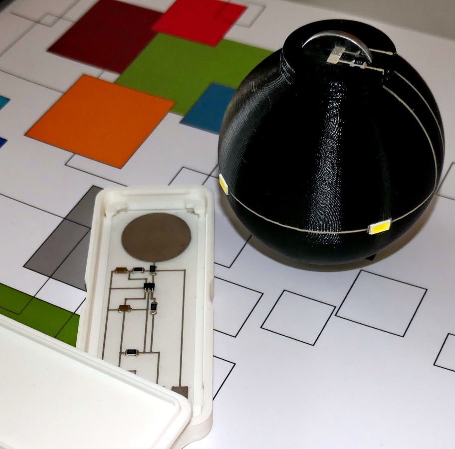
By combining classic FDM (Fused Deposition Modeling) technology with the additive manufacturing of printed electronics and the assembly with SMT components, individualized mechatronically integrated 3D assemblies can be produced on spatial circuit carriers. The process is carried out in a machine with a 6-axis system for three-dimensional processing. In addition to FDM, the piezojet printing process was installed for contactless printing with functional inks and pastes on any 3D geometries and pick & place SMD assembly. Key issues are the reliability, conductivity and contacting of printed structures. Projects include a printed stator for DC micromotors, the functional integration of sensors and antennas in assembly and maintenance systems on aircraft fairings or reliable and automatable connections of printed electronics to the aircraft electrical system.
3D-printed electronics can also be combined with conventional electronics and additive (substrate) manufacturing, emphasized Johannes Hörber from Neotech AMT, an equipment specialist for 3D manufacturing. Application-specific advantages such as flexible design, economical production processes, short process times, reduced material usage and increased reliability are achieved with the 3D printing process. There are also environmental factors such as a lower material mix and quantity, easier recycling and reduced parts tourism. While in conventional PCB production, the production of the conductive track structure (bare PCB), the assembly process of the components, the production of intermediate connections and final preservation or finishing are usually strictly separated, often even in different companies, this can be done simultaneously in any order in the additive process with a complex process module, as Jan Fröhlich already described. Neotech has combined five-axis motion systems with product-specific printing technology for printing electronic structures on 3D MID substrates. Very complex mechatronic devices can be produced with one tool, for example by printing conductor paths on 3D surfaces using different types of jetting processes, piezo jetting of silver paste (line width 350 µm) and nano-jetting with silver ink (line width around 100 µm). A CAD/CAM software tool is adapted that links the design data with production and generates the G-code. Additional print modules were integrated for applying structured metal layers for touch sensors or heating elements. Pick & Place modules and a camera-based system were added for SMD assembly. The direct printing of electrical interconnections to already embedded SMDs is also possible.
 Fabian Ziervogel explained the FDM technology at IWU.He had brought along MID demonstrators from the 3D MID e. V. research association for illustration purposes. Another example mentioned was the combination of the various modules for a 'fully additive' production of a tulip-shaped luminaire with the processes: Mechanical substrate structuring, piezo printing of the silver conductive structure, pick&place of the SMDs, extrusion of transparent TPU protective layer.
The process has also been used for printing conformal antennas for mobile communication and IoT devices or 3D printing on ceramic substrates for electronic applications, such as LTCC-based 3D substrates for sensor and radio components in the automotive sector. The technology has potential for the next generation of mobile technology made from 3D-molded glass. The current focus of applications is on simple printed electronic functions on substrates ranging in size from millimeters to decimeters.
Tool-integrated sensor and actuator systems
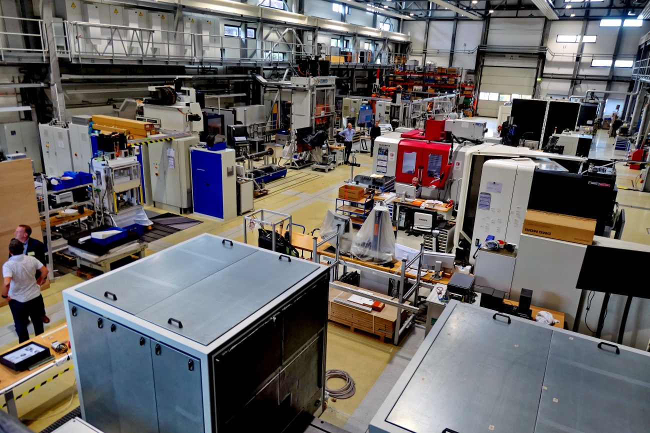
Intelligent production systems require integrated sensors and actuators, digitized interrelationships, robust operation and precise targets. The IWU is working intensively on the development of tool-integrated sensor and actuator systems, explained Wolfgang Zorn, Head of Business Unit at the IWU. The participants of the meeting were able to find out about this work during a visit to the IWU machine hall (technical center).
 We discussed the human-robot relationship with Johannes Weber
 Discussions on tool-integrated sensor and actuator systems as well as mechanical and adhesive joining technologies
There are high demands on the electronic components used for communication (Bluetooth, CAN, EtherCat, ProfiNet) and compatibility with various measuring principles. A 24 V power supply or alternatively battery operation is used. Robustness against production conditions, integrated edge intelligence and system integration are essential.
He described various research tasks, such as the additive ball screw drive, the monitoring and control of milling or forming processes or ultrasonic superimposed drilling.
Sustainability through biopolymers
Daniel Firzlaff from HTW Dresden presented research work on the use of biopolymers in electronics and sensor technology and the technologies used. One focus of the presentation was investigations into special functional layers in humidity sensors. Material developments and modifications demonstrated the potential of biopolymers in terms of sustainability and biodegradability. Additives enabled the successful adaptation to different requirement profiles. For use as a carrier material, the aim is to further improve heat resistance and reduce moisture absorption. I have already reported on this research project in detail in my report from Dresden in PLUS 8/2020 (p. 1108-1114).
Together with the IWU, the organizers of the SAET once again succeeded in organizing a highly interesting and even international (USA) event, which demonstrated very impressively that the development of manufacturing technologies for printed circuit boards is far from over. The production of complete assemblies in a complex machine instead of in long lines or even several factories is still a niche, but an impressive vision of the future. The very competent explanations and demonstrations of laboratory practice by employees of the host Fraunhofer-IWU in their Dresden technical center also contributed to the success of this successful event.
 About the person

Dr. Rolf Biedorf has been writing for Leuze Verlag since 1994 and has been reporting on current events in the Saxon microelectronics scene in PLUS for 10 years. After studying chemistry, he worked in the electronics industry and, in particular, at the TU Dresden in research and teaching in the fields of coating, assembly and interconnection technologies in electronics.
www.avt.et.tu-dresden.de/saet/arbeitskreis
www.iwu.fraunhofer.de
