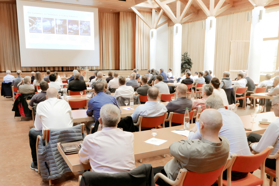
Current trends and new products from the PCB industry were once again presented at this year's 'Traditional PCB Seminar' in Uitikon.
 Romeo Premerlani, organizer of the SGO PCB seminarIf you askedindividual visitors to the traditional PCB seminar of the Swiss Society for Surface Engineering (SGO) why they had come, most of them said that they wanted to be inspired and find out about the latest developments in the PCB industry. The seminar, which this year was once again held at the Uediker-Huus conference center in Uitikon near Zurich, is obviously also an ideal place to make contacts and network.
While welcoming the 70 or so participants, seminar organizer Romeo Premerlani reminded them that the first patent for printed circuits was filed with the British Patent Office in 1943 by an Austrian in exile in London. (see: 'Paul Eisler's life with the printed circuit board', PLUS 9/2023) The invention of Paul Eisler, who was born in Vienna, was not to become established until later, however, because at that time women's work was still cheaper and it was obviously worthwhile continuing to wire the electrical circuits by hand. It was only when the US military industry discovered Eisler's invention and developed it to the point where it was ready for series production that the printed circuit board, which was the center of attention that afternoon in Uitikon, Switzerland, began its triumphant advance in electrical engineering.
"The corona crisis is largely over"
Remo Fischer, Hofstetter PCB
 Remo FischerIn addition tothe specialist presentations, it is a tradition of the SGO PCB seminar that visitors are given an overview of the current market situation in the PCB industry in Europe and the DACH region in particular at the start of the event. Remo Fischer was able to report on a "slight recovery" in the European PCB industry following the coronavirus pandemic. "We are roughly back to the level we were at in 2019. The coronavirus crisis is largely over," said the Operations Manager and Deputy Managing Director at Hofstetter PCB AG in Küssnacht, Switzerland. However, despite overcoming the crisis, the number of European companies in the PCB industry has fallen from 247 to 172 since 2015, while global turnover in the PCB industry has increased since 2015 and also during the pandemic, as Remo Fischer's data presented showed. Fischer expects that the defense sector in particular will continue to grow due to the current situation in Ukraine. In a country comparison, Germany is ahead with the largest PCB industry in Europe. Since the slump in the coronavirus pandemic, turnover at German PCB companies has been rising again, but has not yet returned to 2019 levels. In Austria and Switzerland, turnover in the PCB industry rose significantly above the 2019 level following a slump in 2020.
Supply bottlenecks and recruitment problems
 Hermann Reischer, Polar InstrumentsInthe concluding SWOT analysis (strengths, weaknesses, opportunities and threats), Fischer pointed out that the European PCB industry is strong in the field of prototyping on the one hand, but that there are supply bottlenecks in material procurement on the other. "If the basic material is not available, I cannot produce prototypes," Fischer pointed out the contradiction. Another contradiction in the European PCB industry appears to be personnel. The industry can currently boast well-trained specialists, but could soon be faced with a recruitment problem. "We have a lot to do in the area of junior staff," said Fischer, referring to the PCB industry, which is apparently affected by the general shortage of skilled workers. He called on companies to join forces in the coming years. "The market should not get much smaller. Otherwise it will no longer be able to make a difference," said Fischer.
The presentation following the market analysis dealt with the challenge that materials for PCB production must now also be designed for transmission frequencies in the gigahertz range if they are to be used for electronic components for high-speed internet connections, for example. During his presentation, Hermann Reischer from Polar Instruments in Nußdorf, Austria, which develops software and test systems for printed circuit boards, introduced the measurement method developed by Intel called 'Delta L 4.0'. When developing the high-frequency test method, the developers were faced with the particular challenge that the entire measurement setup has a massive impact on the measurement result. "The connections are a particular problem here," said Herrmann Reischer. The test system developed by Polar Instruments, called 'Polar ATLAS VNA Delta-L 4.0', can test the material suitability of conductors at transmission frequencies of up to 43 GHz, but higher frequencies are already possible: "There is another version of this test system that can test up to 70 GHz. However, we do not yet see a great demand on the market," said Reischer.
Focus on mSAP and biosensors
 Hortense Gaya, CCI Eurolam GroupThomasPliet's presentation focused on the use of mSAP technology (mSAP = Modified Semi Additive Process) to meet the ever-increasing demands on PCB technology - particularly in the mobile communications, automotive and medical technology sectors. According to Pliet, the main challenges here are increasing integration density, better signal transmission and improved heat management on the circuit board. Project manager Pliet, who came to Uitikon as an employee of Max Schlötter from Geisslingen a.d. Steige, explained how the above-mentioned requirements can be met using mSAP. He presented the 'SLOTOCOUP SF 50' copper bath developed by Max Schlötter for the electroplating of printed circuit boards, which can be used to coat inner layers, superstructures and outer layers. According to Pliet, the process optimizes electroplating copper deposition and makes it more efficient.
In her presentation, Hortense Gaya, Head of Printed Electronics and Thick Film Pastes at the CCI Eurolam Group, spoke about the advantages of thick film technology, particularly in the development of flexible and stretchable PCB projects. The technology is used in particular for biosensors, wearables and medical skin electrodes and plasters. In the process discussed by Hortense Gaya, conductive pastes are printed onto substrates made of plastics such as PET, PI or TPU.
Miniaturization of components by up to 70%
The presentation by Valentin Storz, Managing Director of Nano Dimensions' European headquarters in Munich, focused on the use of 3D printing in the development of prototypes and ultimately in the production of electronic components.
The Israeli company's 3D printers use additive manufacturing of electronics (AME) to produce electronic circuits. In this process, components and circuits are produced by applying materials such as conductor tracks, solder joints and electronic components in layers. The use of AME in the 3D printing process developed by Nano Dimensions also makes it possible to produce three-dimensional parts - in contrast to the classic two-dimensional printed circuit board. "Producing not just the electronics, but complete components or products in just one machine and only having to store the data for this," said Storz, explaining the company's vision. Important advantages of the process are that electronic components can be miniaturized by up to 70%, and the technology can also save costs when creating prototypes and reduce development time. "In future, it will be more about what we can produce regionally without having to fly it around the world by plane," said the CEO with regard to the sustainability of his 3D printing process.
 Valentin Storz, Nano Dimensions
 Cyril Voisard, Coat-X
 Honor to whom honor is due: Peter Weber and Hansruedi Fischer
In the last lecture, Cyril Voisard, Coat-X, presented a technology that can be used to coat critical components such as circuit boards, sensors and magnets. The company from La Chaux-de-Fonds in Switzerland uses a coating based on parylene. This can be applied less than 10 µm thick. The biocompatible material can also be used for implanting electronic components into the human body, such as pacemakers, explained Sales Manager Voisard. The Parylene coating is water-repellent and can withstand extreme temperatures of up to plus 125° and minus 55°, according to the sales managers' presentation. However, it is not scratch-resistant, as Voisard explained when asked by the audience.
At the end, Romeo Premerlani paid tribute to his two predecessors Peter Weber and Hansruedi Fischer - who, like Premerlani, were once organizers and presenters of the SGO PCB seminar, which has existed since the early 1980s. The two of them each received a gift basket from him. "They have helped to make this event possible and to ensure that it is so well attended," said Premerlani. The speakers, participants and organizers rounded off the seminar day with an aperitif and then dinner together.
 Relaxed atmosphere: between the breaks there was the opportunity for networking and professional exchange
Pictures
All pictures were taken by Heinrich Sturm (heinrichsturm.de) and made available to PLUS with kind permission
