The KSG Group concluded its three-act 'XPERTS on tour' with an event in Jena. In addition to the presentations at the live event, participants were treated to a galactic evening program in the planetarium - and the most entertaining embedding of a fire alarm imaginable.
KSG announced last year that it would be trying out a new concept instead of a mundane technology day. The fruits of this idea were three events in Linz, Dortmund and Jena. (The PLUS reported on this after the last 'electronica' in issue 12/2022).
The 'XPERTS on tour' program was explicitly aimed at existing and new customers of the PCB manufacturer - some companies were also specifically approached and given an invitation. According to Katharina Luchner, Head of Marketing at KSG, each event was characterized by its own dramaturgy and atmosphere.
dramaturgy and atmosphere. The number of visitors - in all three cities combined - was 90 people ... a thoroughly exclusive event that actually deserved to be more popular. Nevertheless, the PLUS editorial team was able to attend the finale in the Volkshaus Jena.
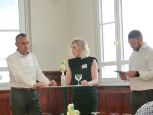
 Swen Klöden in an interview with his employees'XPERTS on tour' washostedby Katharina Luchner and David Müller, Head of Sales at KSG. The duo first interviewed CTO Swen Klöden, who has been managing the company alongside Margret Gleiniger since 2020. Klöden gave a review of the past few years - a difficult time for KSG, not only because of the Covid pandemic and the slump in the automotive sector, but also due to the need to 'catch' soaring energy costs. Klöden reported with great emotion how the management had moved its work area to production in order to set an example in terms of saving energy. They had tried to "set an example of normality". This had brought the workforce together and aroused emotions. During the changeable period, the medical technology sector in particular experienced an upturn (e.g. ventilators). This has made the company aware of the social significance that a PCB manufacturer can have. As an outlook for 2024, Klöden mentioned the planned commissioning of a chem. NiAu plant, the increased use of A.I. in final testing and furtherCO2 savings of up to 40% as part of sustainability.
Facilitated design automation in electronics development
Matthias Stickl (KSG) and Alexander Pohl (Celus) then reported on the collaboration between their companies to optimize customers' electronics through digital processes. The focus was on the Celus Design Platform, which is intended to take effect even before EDA tools in the concept phase, when simple Office documents and scripts are used on the 'virtual drawing board'. This is where the Design Platform comes in and aims to support the design process with 'intelligent algorithms' and A.I. processes so that, according to Alexander Pohl, a prototype including cost calculation can be created within minutes.
Matthias Stickl, on the other hand, listed digital optimization options, such as the simulation of copper deposition in the pattern plating process using a 'digital twin' - comparable to the Elsyca tool that Dr. Agniezka Franczac impressively presented in PLUS 8/2023. However, the symbiosis of Celus and KSG was not really tangible in the presentation, as the presentation sections were suboptimally intertwined. This was followed by skeptical questions from the audience - there is a desire among customers for better data exchange, but not in such an abstract way.
Base material accounts for the lion's share of manufacturing costs
The next presentation 'Road to Reduction' by Uwe Kieshauer, Area Sales Manager of the KSG Group, was more convincing. He gave tips for the
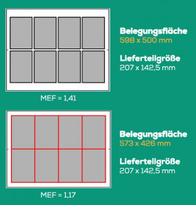
cost-optimized printed circuit board and focused on the 'lion's share' of manufacturing costs: The base material and its processing (pressing, drilling, milling), especially in view of the sharp rise in the price of copper (see 'Scarce copper', PLUS 10/2021). This item accounts for 35% of LP production costs, which is why optimal material utilization has an impact on all process costs. Tolerances should be planned as tightly as possible and, in contour processing, the same delivery part size can be achieved with a smaller surface area by scribing instead of milling. Kieshauer recommended reducing the number of layers ("Saves time and money") and warned against expensive and complex internal contacts, buried vias and single-ply structures.
 Scoring instead of milling improves material utilizationTheproblem with single-ply structures, according to Kieshauer when asked, is mainly due to the lack of resin content to fill the 'peaks and valleys' in the affected inner layer. The prepregs are not just the insulation layer: the resin that flows during the pressing process fills the etched-out areas and encases the conductors, so it is also the 'adhesive' for the bond. Using only one prepreg (single ply) quickly reaches the limit of the required resin content. Nevertheless, due to the maximum possible aspect ratio (circumference of the hole to depth) of 1:0.9 for laser micro vias - i.e. for lasered blind holes - no other structures than single ply are possible; the thickness of two prepregs would exceed the possible AR. However, it would then be necessary to ensure the largest possible copper surface on the inner layer so that the resin can fill sufficiently. This explains Kieshauer's skepticism about single-ply structures.
The lecturer had a saying for the cost optimization of drilling and milling processes: The "thickest sandwich" is the best - it is important to make the drill hole diameters as large as possible and reduce their number. Kieshauer also gave a number of tips for the application of anti-corrosion coatings, advised against color variants beyond the classic green tone (unless technically necessary, for example for special reflective behavior of visible PCBs) - and concluded with an appeal to customers to involve the PCB manufacturer as early as possible in order to achieve cost savings.
The subtext of Kieshauer's words was clear: although PCBs from the Far East may be cheaper on paper, clever planning and consideration can lead to significant cost advantages if a local manufacturer is consulted at an early stage, i.e. in the case of domestic production ... and ultimately the better PCB, the better product. Without saying it directly, Kieshauer conveyed this idea in his very precise and well-structured presentation - the highlight of the day, which thematically, programmatically and ideally went far beyond recommendations to KSG customers.
Broad portfolio of HDI printed circuit boards
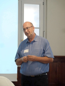
 Uwe KieshauerThomasDoberitz, Technical Support KSG, was left to enumerate the production possibilities of the PCB manufacturer. KSG is undisputedly one of the most important German PCB companies: In the NTI 100 Report 2022, the Gornsdorf-based company is ranked 109th (closely followed by Schweizer Electronic, ranked 110th; well ahead of both Würth Elektronik, ranked 80th, see PLUS 10/2023).
Accordingly, KSG's portfolio offers all variants of HDI PCBs, a variety of microvia arrangements (buried vias, i.e. 'buried' vias inside the HDI structure; staggered or stacked through-holes for all connection paths) - in short: there is virtually nothing that KSG does not offer. Customers are advised to use an 'HDI checklist' to check which vias they actually need, which drill holes are required on which layer and which closure technologies make sense. Doberitz recommended following the credo: 'As fine as necessary, as generous as possible' when laying out a PCB.
He was, of course, contradicting Uwe Kieshauer's admonition to 'economize' on materials - as Doberitz himself admitted. Overall, his presentation was dominated by the enumerative character, and one would have wished for a more concentrated presentation.
Surprise break in the September sun
The finale provided some amusement: Thomas Brenner, penetration tester in the areas of web, mobile and embedded security at T-Systems Multimedia Solutions (Telekom), reported on his everyday life as an IT forensic expert. Very few people were aware of just how dramatic the security situation is for Internet users: the simple tricks used by sinister identity thieves and data hijackers to gain access to our software and online accounts was shocking; and the low prices at which gadgets for hacking telephones, car doors, hotel room door cards or fire alarms can be purchased on the Dark Net or simply on eBay was a source of trepidation.
It was therefore fitting that 'XPERTS on tour' had to be interrupted at short notice: a fire alarm forced the participants to vacate the Volkshaus for half an hour. Outside in the September sun, there were smiles until the 'false alarm' message made it possible to return - everyone suspected that Thomas Brenner had played a joke with his gadgets. Of course, he vigorously denied this (but clearly enjoyed the fact that he was believed to have pulled off such an ingenious coup).
The event was rounded off with an impressive visit to the Jena Planetarium and dinner. The KSG crew could sit back and relax: The last 'XPERTS on tour' date also met with the approval of the interested visitors. According to Katharina Luchner, it will be announced in due course whether the series will continue - and if so, at which locations.
www.ksg-pcb.com
www.celus.io
www.t-systems.com
http://schutzschild.info/


