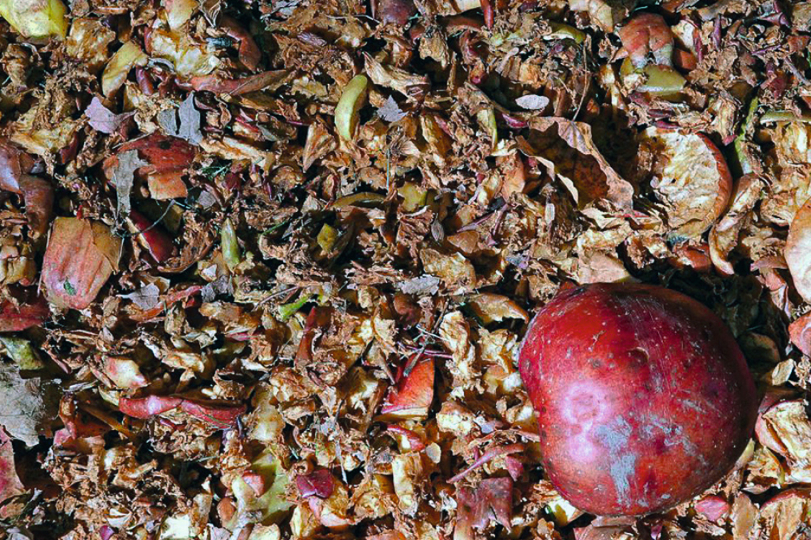
It is now once again known for tourism, juicy apples and a flourishing timber industry: the Kashmir Valley in northwest India. The current industrialization is taking different forms. Apple pomace and sawdust are two important agricultural wastes produced in this valley. A group of researchers from the renowned Indian Institute of Integrative Medicine Jammu and the agricultural university SKUAST-Kashmir worked together to investigate how this waste can absorb the toxic heavy metal cadmium. Worm compost made from apple pomace and sawdust was made and converted into biochar and studied.
Cow dung, which was pre-composted for 21 days, was mixed with apple pomace and sawdust in varying proportions. The team used the earthworm Esenia fetida and mixed the compost every 15 days to ensure good aeration. Moisture and pH levels were maintained throughout the composting process. The so-called apple pomace-based vermicompost resulting from the worm compost was harvested after 45 days, the sawdust-based vermicompost after 60-65 days. The researchers then dried, ground, sieved and pyrolyzed the compost to produce biochar. The adsorption of cadmium was investigated at pH 2 and pH 8. Among the various adsorbents, the maximum adsorption (35.075 mg.g-1) was determined according to the Langmuir adsorption isotherm for so-called vermicompost made from 100 % sawdust. Among the biochars, the maximum adsorption (3.0 mg.g-1) was determined for biochar from 100 % apple pomace. All adsorption systems were exothermic, with AT values between 0.05-0.75 J.mol-1 at pH 8 and 0.118-0.485 J.mol-1 at pH 2. Adsorption was more efficient at higher pH values due to deprotonation of functional groups and electrostatic interaction. About 83 to almost 100 % of the cadmium could be removed in the course of 1-3 hours, depending on the condition. In general, the conversion of vermicompost into biochar improved cadmium absorption. This could be due to the higher porosity and better access to the functional groups that adsorb cadmium from the water. The use of vermicompost and the resulting biochar is a multi-layered adsorption process and can be used to decontaminate affected sites. Adsorption could be completed in an optimal time frame required for industrial application to treat contaminated water on a large scale.
Chem. Ecol. 2024, DOI: 10.1080/02757540.2024.2320888
 und Verschleißspurprofil der mit HVAF gespritzten WC-10Co-4Cr-Beschichtung (rechts). Zum Vergleich ist auch die Leistung einer HCP-Beschichtung ähnlicher Dicke angegeben.") Fig. 2: SEM image of the interface (left) and wear track profile of the WC-10Co-4Cr coating sprayed with HVAF (right). The performance of an HCP coating of similar thickness is also shown for comparison.
Fig. 2: SEM image of the interface (left) and wear track profile of the WC-10Co-4Cr coating sprayed with HVAF (right). The performance of an HCP coating of similar thickness is also shown for comparison.
Cermet coatings using HVAF as a hard chrome plating replacement
HVAF (High Velocity Air Flame Spraying) is a relatively new process for spraying high quality coatings of metals, alloys, carbides and borides onto metallic surfaces. Coatings with fine powders (5-15 µm) can be applied. Scientists from ARCI, an autonomous body of the Department of Science and Technology (DST) of India, along with engineers from the Indian Institute of Bombay, have synthesized thin hard coatings of a composite alloy of tungsten, cobalt and chromium (WC-10Co-4Cr) using HVAT and developed it into an alternative to hard chrome plating. The thin films were deposited with multiple torch options and using different nozzle sizes to better understand the role of different combustion heat fluxes and velocities on the overall characteristics of the thin cermet films. A detailed microstructural characterization was performed to correlate the sliding wear performance of the sprayed thin films with the phase properties. A comparative study with hard chrome plating evaluated the performance of the sprayed cermet thin films.
The surface roughness of the thin thermally sprayed WC-10Co-4Cr coatings was an order of magnitude higher than that of hard chrome plating, but lower when compared to coatings deposited with conventional particle sizes. Coatings with a thickness of 50 µm and a surface roughness of almost 1.5 µm were achieved on stainless steel substrates. The coating can be deposited in an unprocessed state to achieve a smooth surface and a layer thickness of around 50 µm. This significantly reduces the post-processing steps after coating, which considerably reduces processing and raw material costs and offers better wear resistance than HCP. As expected, the torch type and nozzle design had a significant influence on the coating properties. The thin WC-10Co-4Cr coatings produced by HVAF showed better sliding wear performance compared to conventional hard chromium coatings (HCP). Corrosion studies carried out on the coating and compared with HCP also showed that the new technique can be a better alternative to HCP for heavy-duty applications such as hydraulic shafts, valves, piston rods or balls. The advantages of using fine powders include lower porosity and crack-free coatings. The results of this study provide insight into the optimum thermal energy required to avoid excessive melting and/or oxidation of the surface while maintaining dense microstructural properties through sufficient kinetic energy for improved wear resistance.
J Therm Spray Tech 32, 904-917 (2023). https://doi. org/10.1007/s11666-023-01563-9
Semiconductor and electroplating solutions
NEPES Corporation is based in Cheongju, South Korea, and is a global provider of wafer level packaging, panel level packaging and turnkey assembly solutions including test and DPS services. The company recently announced that it will start mass production of electroplating solutions locally this year. These are electroplating baths, which are essential for semiconductor chips to maintain their electrical properties while increasing their density. Until now, these have been sourced exclusively from foreign companies in Japan and the United States, according to a company press release. NEPES has now reported that the coating solution it developed has been adopted by semiconductor memory manufacturers for Through Silicon Via (TSV) in a High Bandwidth Memory (HBM) process. In the TSV process, memory chips are stacked vertically and electrical signals are transmitted between them, which is crucial for HBM production. The newly developed products will not only be suitable for HBM, but also for semiconductors with a microscopic process of 10 nm. The company expects sales of around 33 million US dollars this year. Thanks to the growth of high-performance D-RAM semiconductors and semiconductors for artificial intelligence (AI), sales of this product are expected to grow at a high rate of more than 30-40% per year.
https:// www.chosun.com/english/industry-en/2024/04/04/CIIH4YZX65EFRGT232LYJYBSQU
