Organic light-emitting diodes (OLEDs) and photovoltaics (PV) have gained a firm place as renewable energy sources. Unfortunately, they are susceptible to damage under hot and humid environmental conditions, especially in tropical countries. Conventional PMMA or PMMA-polyolefin based semiconductor coating materials offer limited protection due to their permeability to moisture/oxygen and the formation of cracks during prolonged exposure to the environment. Therefore, there is an urgent need to improve the existing self-healing coating materials with properties such as high water/oxygen barrier, mechanical flexibility, optical transparency and self-healing properties.
Researchers at the Indian Institute of Technology (IIT) Bhilai in the state of Chattisgarh ("thirty-six forts") have taken a crucial step in producing a cost-effective and industry-friendly formulation for a "self-healing coating" for solar cells. The researchers have developed a simple approach to redox-sensitive self-healing coating materials by in situ cationic block copolymerization of styrene and 2-chloroethyl vinyl ether. The process is based on sequential "water-tolerant" cationic polymerization and subsequent post-polymerization modification, leading to the synthesis of a redox-sensitive and self-healing coating material based on polystyrene-block-poly(2-thioethyl vinyl ether) diblock copolymers. To optimize the reaction parameters, FeCl3/nBu4NBr-mediatedcationic polymerization of styrene was carried out under "open air" conditions as well as under "dry" conditions with different combinations. This new method enables the spontaneous "healing" of cracks within only 5 minutes, offering a promising solution to repair damage caused by hot and humid ambient temperatures (Fig. 1). The introduction of this self-healing coating material prevents the propagation of cracks and restores the material and system properties. Further evaluation and testing of this new technology is underway. https://doi.org/10.1016/j.eurpolymj.2023.112251
 Fig. 1: Indian scientists have now developed a "self-healing" coating method for semiconductor coatings based on PMMA or PMMA polyolefin
Thin film corrosion protection
Various strategies are being developed to either prevent or slow down the corrosion process in materials. One widely used method is to cover the surface with a functional, thin layer. Over the decades, methods such as chromate-free coatings, sol-gel coatings with nanoparticles, multilayer coatings of alumina, titania, tantalum oxide and alumina-titania, copper with diamond-like carbon (Cu-DLC) and plasma polymerization have been used. These have been summarized in a short paper by Samudrapom Dam.
https://www.azom.com/article.aspx?ArticleID=22882
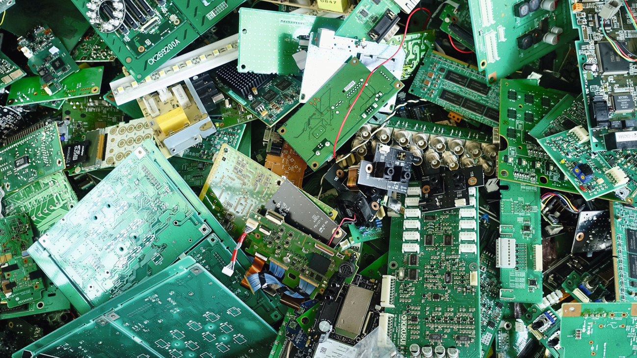
Recycling of e-waste
It is estimated that India generates more than 3.2 million tons of used electronics every year. E-waste is a huge challenge for the environment (Fig. 2). The Hyderabad-based Centre for Materials for Electronics Technology (C-MET) is an independent, public R&D center in the field of electronic materials. Many projects are carried out in a public-private partnership. The center has developed innovative recycling technologies for printed circuit boards, lithium-ion batteries, permanent magnets and silicon-based solar cells. The environmentally friendly recovery of valuable metals such as copper, silver and gold from obsolete circuit boards has been optimized in a demonstration plant with a capacity of 100 kilograms of circuit boards per day. Processing facilities such as deslagging, shredding, melting, remelting, electrowinning and leaching with gas purification systems were set up to meet environmental standards. A front-fired, low-cost rotary tilting furnace was developed locally to mechanize the smelting process and thereby improve yields. The process developed by C-MET produces silver with a purity of 2N, around 90% pure copper and 99.9% pure gold. A recycling plant for printed circuit boards was recently opened, which can process one ton of material per day. Meanwhile, Re Sustainability Limited is ready to commission Asia's first certified e-waste and industrial scrap processing plant in Hyderabad. The plant, with an annual capacity of 20,000 tons, is being set up in a 51:49 joint venture with the US company Reldan. The joint venture company Re Sustainability Reldan Refining Ltd. will invest money in several phases to set up an integrated e-scrap recycling plant. The plant will feature advanced technologies for the recovery and refining of precious metals and will be an important step towards a sustainable circular economy for e-waste. Current PCB recycling processes can be divided into two categories depending on the technology used to recover the material, namely thermal and non-thermal processes. In thermal processing, hydration, pyrolysis and metallurgical processes are used after separation. In non-thermal processing, chemical treatment, dismantling, separation and comminution techniques are used. The result of the non-thermal processes is usually subjected to additional chemical treatment. Most current recycling processes only recover around 28% of the metal content of PCB waste. Over 70% of PCB waste cannot be efficiently recycled or recovered and must be incinerated or landfilled.
