Temperature-dependent deformations of substrates and components as joining partners of electrical assemblies can be the cause of undesired field failures. An early analysis option is dynamic topography measurement, in which the topographies of components and assemblies can be measured under temperature load in a stress-free and assembled state. The article discusses the basic causes and typical fault patterns for selected examples. The potential for accompanying measurements in the context of product development is also demonstrated using the example of an antenna module.
Temperature-dependent deformations of substrates and components as joining partners of electrical assemblies can be the cause of undesired field failures. An early analysis option is provided by dynamic deformation measurement, which can be used to measure the topographies of components and assemblies under temperature load in a stress-free and assembled state. The article discusses the basic causes and typical failure patterns for selected examples. An example of an antenna module is used to demonstrate the potential for accompanying measurements as part of product development.
1 Motivation
The variety of shape, size and function of electronic components as well as almost unlimited possibilities in the design and layer structure of circuit carriers leave hardly anything to be desired for the design of assemblies and for downstream electronics production, but also harbor some risks in terms of processing and reliability. For example, PCBs and components with heterogeneous layer structures and material compositions are used in the surface mounting of electronic assemblies. The materials used - polymers, metals, ceramics, etc. - have different thermal expansion coefficients. Under thermal stress, such as soldering during component assembly or under field conditions due to self-heating caused by power losses and/or external temperature changes, this leads to a change in shape. These deformations appear as twist and/or bow and are generally summarized as warpage. Figure 1 illustrates these aspects using the example of warpage for a printed circuit board and a component in the de-energized state and for the assembled state. The latter (bottom right in the figure) means that the arrangement is in a state of force equilibrium and the amplitudes are lower than in the de-energized state, but the components and the solder joints are under mechanical stress.
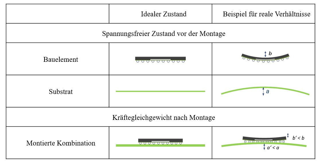 Fig. 1: Temperature-dependent curvature for the stress-free and equilibrium stateInaddition to contributing directly to soldering errors or the shaping of solder joints during assembly, the temperature-dependent curvatures can also pose a reliability problem due to these "frozen" stresses. In this case, mechanical or thermo-mechanical stresses occurring in the field can lead to earlier fatigue of the solder joints and thus have a negative impact on the service life. Examples of quality defects in the form of soldering faults that are clearly related to the bending of the joining partners can be divided into the following categories:
![Abb. 2: Potentielle Lötfehler aufgrund von Verbiegungen (eigene Darstellung in Anlehnung an [1])](/images/stories/Abo-2023-06/thumbnails/thumb_Abbildung_02.jpg) Fig. 2: Potential soldering defects due to bending (own illustration based on [1])Open solder joints
Fig. 2: Potential soldering defects due to bending (own illustration based on [1])Open solder joints- Short circuits
- Uneven standoff
- non-conforming shape
- Pad breaks.
Possible soldering defects for a BGA package are shown in Figure 2.
Knowledge of the temperature-dependent bending of the joining partners is therefore an important acceptance criterion for the development and use of electronic components and assemblies. They are therefore of great interest in order to identify sources of production errors and to gain a deeper understanding of the reliability behavior of an assembly. Since the early 2000s, three trends have increased the need for temperature-dependent bending measurements. These are the trend towards components with smaller pitches, the increased soldering temperatures in the lead-free process and changes in the form factors of components. Deflection measurement has become an important measurement method for analyzing, preventing and predicting connection errors and is used in failure analysis laboratories and production facilities worldwide.
2 Measuring principles
Various scanning and imaging methods exist for measuring the topography of a sample. Scanning methods can be both tactile and optical. With sophisticated additional equipment, it is even possible to carry out measurements on temperature-controlled samples above and below room temperature. For the objective pursued here, however, a 'real' dynamic topography measurement is necessary. This means that the sample to be measured must be able to be exposed to temperature profiles that are at least very close to the respective application and it must be possible to continuously measure its behavior. The latter point significantly defines the requirements for the measurement method, which can only be guaranteed by optical methods. Figure 3 shows a comparison of the measuring principles.
 Fig. 3: Comparison of different measuring principlesIn principle,there is a wide range of different optical measuring methods for 3D shape detection. These methods are based on three physical measuring principles: the geometric principle, the time-of-flight principle and the radiometric principle. In optical 3D measurement technology, methods based on the geometric principle predominate and the principles of structured light and combined with triangulation are used in a large number of applications. Here, the phase-shifting Moiré methods play a dominant role due to their high achievable measurement accuracy, spatial resolution and data density.
A common method [2] for the bending measurement of components and printed circuit boards is the use of the shadow moiré technique in combination with a heating chamber (TherMoiré). In the shadow moiré method, the same grid is used for projection and observation, which must be positioned close to the object surface. However, this arrangement limits the lateral resolution and the measuring range in the z-direction and does not allow the measurement of steps and discontinuities.
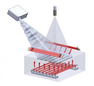 Fig. 4: Principle of fringe light projection in the measuring systemVirtualmoiré or fringe projection representafurther development. In the phase shift method, patterns of gray value progressions of equidistant stripes are sinusoidally modulated, projected onto the sample surface and recorded directly with the camera without optical overlays of a reference pattern. These regular fringe patterns are distorted by the current topography of the sample. The superimposition with a reference structure for the pixel-precise calculation of the relative vertical deflection is then software-controlled [3]. The elimination of a physical grid results in various advantages for lateral and vertical resolution, the measurement of steps, solder balls and discontinuities as well as double-sided temperature control. The TDM Compact 2 measuring device from Insidix is used for such measurements at the Center for Microtechnical Production (ZmP) at TU Dresden. The measuring principle is shown in Figure 4. The sample is placed in a sample chamber, which can be heated and cooled on both sides, as it passes through the set temperature profile. Of course, only temperatures above room temperature are relevant for simulating the changes caused by soldering, for example. For reliability considerations, however, it is of interest to simulate the typical temperature change profiles used in accelerated ageing. This is possible with the aforementioned system by means of an additional option that can also generate temperatures in the minus range in the sample chamber. Some parameters of the system are listed in Table 1.
Temperature range |
-65 °C ... +300 °C |
Temperature ramp |
<= +/- 3 K/s |
Measuring accuracy z |
<= 1 µm |
Repeatability |
approx. 1.5 µm or 2% of the measured value |
Max. Sample size |
300 x 200 mm² |
Depth of field |
up to 25 mm |
(Four different projection and camera lenses can be used to set different combinations of achievable resolution vs. field of views). |
|
Tab. 1: Features of the TDM Compact 2
3 Typical sequence of a complete evaluation
The ZmP at TU Dresden has many years of experience in the field of dynamic topography measurement, but until the end of 2021 this was only possible in the temperature range above room temperature due to the existing system technology. With the measurement technology now available, not only are measurements below room temperature possible, but the preparation effort has also been significantly reduced and the evaluation of the measurement data, including its visualization, has become much more convenient.
For a complete investigation of an issue, it is nevertheless necessary to provide a large amount of additional information or to determine it using measurement technology. Only in this way can as many influences as possible be recorded and taken into account in the evaluation when searching for the causes of faults or investigating reliability-relevant phenomena.
A typical sequence of a complex investigation is as follows (here using the example of a component):
- Recording the basic data (component shape, geometric data, data sheet, component images, batch information, ...)
- Measurement of the component geometry from the top and bottom side using optical profilometry (e.g. laser scan) at room temperature
- Optional: Preparation of the component
- Creation of the measuring environment
- Dynamic topography measurement with application of the temperature profile
- Optional: Repeat measurement on the same object
- Optional: Comparative measurement on identical objects
- Evaluation of the measurement data.
Step 3 is only necessary in exceptional cases if the surface of the sample would influence the fringe light projection too much due to its reflective properties.
Step 4 involves defining and testing the temperature profile for the measurement. It is particularly important to carefully select the temperature measuring point(s) that are available for single or double-sided control. In principle, excessive temperature differences between the top and bottom sides should be avoided.
Step 6 makes sense when investigating production errors, for example if multiple soldering can occur. An object in which stresses were temporarily frozen during its actual production often behaves completely differently in the first reflow soldering cycle than in a second cycle. Multiple cycles are of course also of interest for reliability considerations.
Step 7 primarily serves to rule out the possibility that the behavior of the sample is only exemplary and would be different for other components of the same batch, for example.
Step 8 involves defining the area of the object to be measured or evaluated. For example, some areas that protrude from the "normal" sample surface must be masked in the software so that their measured values do not distort the overall picture.
4 Evaluation options
The recorded measurement values are available as a point cloud with absolute height values and can be visualized as 1D, 2D or 3D representations for each measurement time. Figure 5 on the left shows an example of this for a 'real' printed circuit board. The color scale shows height differences of 300 µm between different areas of the PCB. On the right, a special test PCB with a chessboard-like pad pattern has been measured. Any height profiles can also be derived from such a representation (see marking in Fig. 5 bottom right and profile in Fig. 6). In addition, summary data such as the course of the coplanarity deviation over time (or over the temperature curve) can of course be displayed.
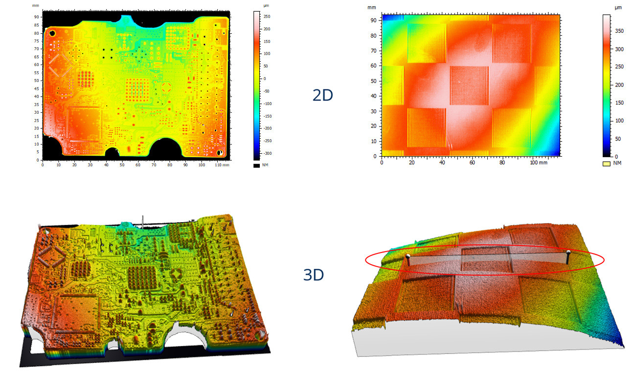 Fig. 5: 2D and 3D representation of the topography at a specific point in time
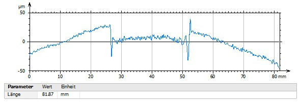 Fig. 6: Elevation profile with reference to Figure 5 bottom right
5 Example of measurement results
In the following, a few examples are given of the phenomena that can occur and how these were investigated using measurement technology.
5.1 Example 1: BGA with head-in-pillow errors
A BGA 272 (pitch 1.27 mm; size 27 x 27 mm²) was analyzed. When mounted on an assembly, a SAC305 solder paste with a wet film thickness of 120 μm was printed, then assembled and reflow soldered. With this BGA, head-in-pillow errors occurred in a real assembly. Figure 7 shows the errors that occurred on a disassembled component, which is not an individual example. The average error percentage was approx. 10 %.
 Fig. 7: Example BGAs with marked solder balls on which a head-in-pillow fault occurred (left package desoldered / right X-ray radiography)
Various scenarios are conceivable for the development of this defect pattern, including poor wetting properties. In this case, however, it was suspected that topographical changes in the joining partners during soldering could be the cause. In this case, the specific BGA ball and the associated pad on the PCB would have to move away from each other during soldering, but then largely return to their original position once the solder has solidified.
A corresponding measurement was able to confirm this suspicion. The measurement was carried out from the top side of the component. Figure 8 shows the two diagonals across the component body at room temperature, at 220 °C (heating, melting temperature of the solder paste) and at peak temperature. At room temperature there is hardly any bending, which can initially be seen as positive. During melting, the coplanarity deviation is approx. 180 μm and at 245 °C it is 260 μm, i.e. more than the limit permitted by the associated standard JEDEC SPP 024 [4]. The BGA curves convexly, i.e. the center of the component rises. This correlates with the error coordinates of the head-in-pillow errors in Figure 7[5].
 Fig. 8: Diagonal profiles of the BGA at different temperatures (x-axis diagonals in mm / y-axis heights in μm)
5.2 Example 2: DCB substrates
DCBs are particularly important substrates for power electronics. Warping and/or twisting are also normal for these objects. When measuring these substrates, it should be noted that the measurement should be taken from the unstructured side, i.e. usually from below. The structures on the upper side very often have step heights of more than 250 µm and can sometimes cause artifacts during measurement due to differences in reflection. However, the structured side can also be measured through targeted preparation. However, there is an increased effort in the evaluation of the surface of interest if the etching trenches have to be masked out mainly manually. This is necessary if the amplitude of the bending exceeds the depth of the etch trenches. Figure 9 shows such an extreme example and the influence of the masked evaluation.
 Fig. 9: Heavily bent DCB (left unmasked / right masked)
In the case of DCBs, it cannot be assumed that these substrates will return to their original geometry after soldering. It should also be noted that substrates often come from different manufacturers. Figure 10 shows a comparison of four DCBs with the same layout and a size of 35*24 mm² from four different suppliers.
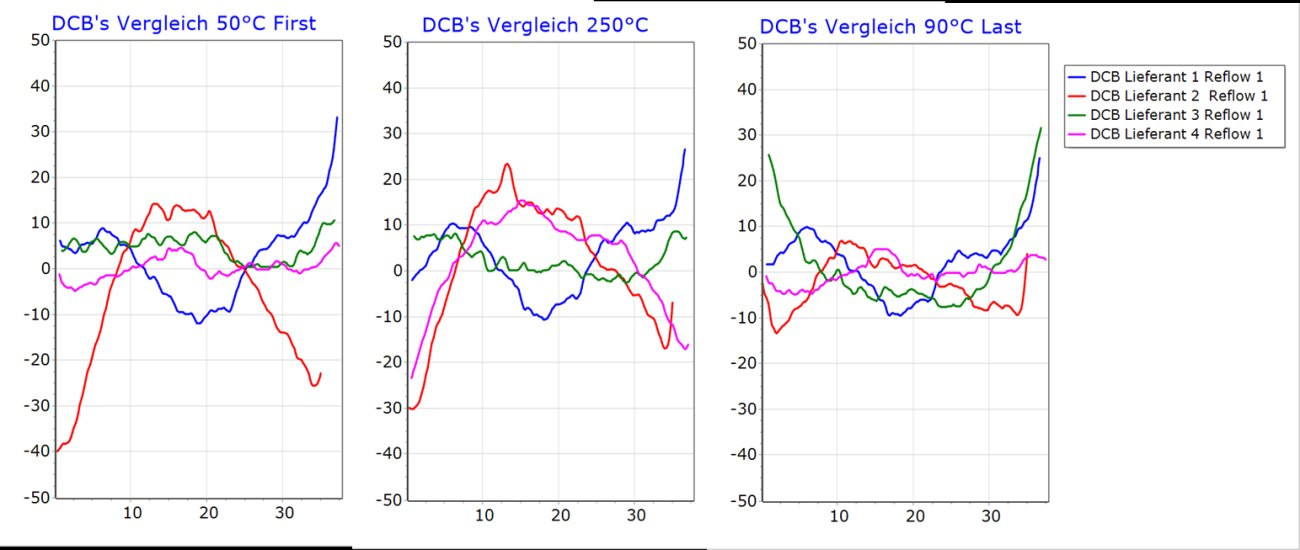 Fig. 10: Measurement on DCB substrates with identical layout but from four different manufacturers
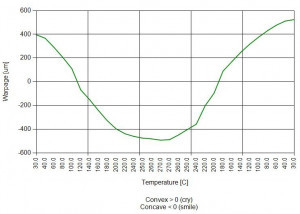 Fig.11: Extreme coplanarity curve of a DCB during a soldering processAlthoughthe curvature behavior of all substrates is not critical in terms of size, clear differences are visible, especially in the temperature-dependent curve. The substrate from supplier 1 (blue curve) shows a continuous concave bending with only slight changes. The substrate from supplier 2 (red) shows the greatest bending (convex) in the initial state, which changes only slightly up to the peak. At the end of the soldering process, this substrate is almost flat. The substrate of supplier 3 (green) shows the opposite behavior. At the start of soldering and at peak temperature, the substrate is relatively flat, only to bend as it cools. The substrate from supplier 4 (purple) shows the greatest bending at the peak temperature. This DCB returns to its initial geometry as with supplier 1, but the direction of bending is reversed. The causes of these differences are probably to be found in the manufacturing technology of the DCBs with the associated internal mechanical residual stresses. DCBs differ greatly in their bending behavior. The amount of coplanarity deviation during a soldering process can easily reach 1 mm (see Fig. 11). It should also be noted that many effects only occur when the DCBs are soldered to a heat sink. Figure 12 shows an example. It should be noted that this combination was almost flat at 200 °C.
 Fig. 12: Extreme curvature of a DCB after soldering onto the heat sink
5.3 Example 3: Antenna module / assembly and temperature cycling test
In the design and development phase of new components, the consideration of reliability at component level plays an important role. During the production of a component, it generally experiences several thermo-mechanical stresses. It can be assumed that the bending state will change several times in succession. An example of the construction of a radar antenna module is used to illustrate these influences. The antenna module studied follows the concept of an interposer-like antenna board, which on the one hand carries the radar antenna array, but also later connects the package to a printed circuit board in BGA style. The signal processor and the antenna driver ICs are housed in a fan-out package at wafer level, which is mounted on the antenna board as a BGA package on the land side. In order to quantify the bending behavior, dynamic topography measurements were carried out on the test assemblies for the successive soldering processes. Three soldering processes are required before the antenna module can be mounted: (1) balling of the antenna module, (2) radar chip mounting and (3) PCB mounting. Figure 13 shows the structure of the antenna module from the soldering side and the finished system assembly.
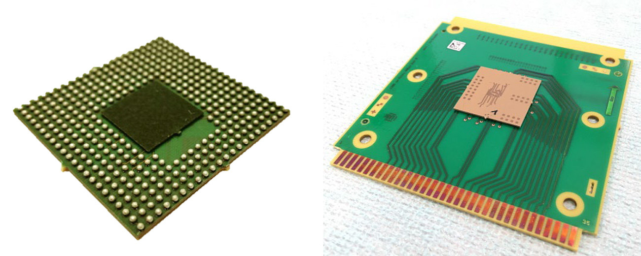 Fig. 13: Antenna module with radar chip from the soldering side (left) / system assembly with antenna module (right)
The dynamic topography measurement of the antenna module was carried out for all simulated soldering processes from the top and solder side, with the analysis of the solder side providing the most important information. In general, an inverse bending behavior would be expected. This assumption could not be confirmed for this complex module. The summary of the measurement results shows a standard-compliant (JEDEC SPP-024) and reversible coplanarity in the stress-free state for all three soldering simulations. The orientation of the coplanarity deviation was determined from the top side. The antenna modules therefore also show a continuous convex bend. The offset of the measured values of the second soldering simulation can be explained by individual differences in the samples, which were produced in the laboratory as a small series.
 Fig.14: Curves of the coplanarity deviation of the antenna module in three soldering simulations
In the following sequence, the system assembly was measured and analyzed. After assembly, the antenna module shows a concave orientation, which is the preferred shape with regard to lower solder joint voltages. It follows the predominant bending of the system board, which is in contrast to extensive investigations on molded components. The coplanarity deviation of the antenna module remains the same in its orientation during a subsequent temperature change and changes only slightly in amplitude, basically following the behavior of the system board. The curves of the coplanarity deviation for the antenna module and the system board are shown in Figures 15 and 16 [6].
 Fig. 15: Coplanarity deviation of the antenna module during temperature changes
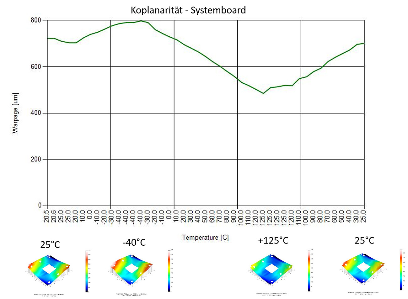 Fig. 16: Coplanarity deviation of the system board during temperature change
6 Conclusion
It has been shown that dynamic topography measurement is both a suitable and important method for diagnosing the causes of faults, but also for the preventive investigation of potential sources of production faults and/or limitations in the reliability of electronic assemblies. With the use of thermally robust optical full-field measurement methods, such as phase-shifted moiré projection, topography measurements can be carried out in a temperature-controlled measuring chamber on individual joining partners as well as on fully assembled modules. The available temperature range covers common soldering profiles. With an additional cooling option, reliability-relevant information can also be obtained as part of temperature change tests. The resulting data records can be processed and analyzed according to any task. This includes profile sections, representations of diagonals and center lines and, of course, 2D and 3D representations for individual images as well as for entire measurement series. Of particular importance is the correct definition of the reference plane for the respective analysis as well as knowledge of surface anomalies that can distort the measurement result. Especially for the use of price-intensive, flat components and/or substrates, bending measurement is an important tool in the context of product development for increasing product quality and reliability.
Literature
[1] W.K. Loh, R. Kulterman; T. Purdie; H. Fu; M. Tsuriya: Recent trend of package warpage characteristic, ICEP-IAAC 2015 - 2015 Int. Conf. Electron. Packag. iMAPS All Asia Conf., 2015, pp. 233-238, doi: 10.1109/ICEP-IAAC.2015.7111029
[2] JESD22-B112A, Package Warpage Measurement of Surface-Mount Integrated Circuits at Elevated Temperature, ©JEDEC Solid State Technol. Assoc, no. May 2005, 2009, pp. 1069-1072
[3] M. Zacher: Integration eines optischen 3D-Sensors in ein Koordinatenmessgerät für die Digitalisierung komplexer Oberflächen, Dissertation, RWTH Aachen, 2003
[4] JEDEC SPP-024, Issue A: Reflow Flatness Requirements for Ball Grid Array Packages, JEDEC Publ., no. 95, 2009, pp. 3.24-1
[5] H. Wohlrabe; K. Meier; O. Albrecht: Effects of warping and warping during soldering on the quality and reliability of solder joints, no. Final report IGF project no. 19468BR, 2020, p. 130
[6] O. Albrecht et al.: Warpage measurements to support the development of mmWave modules, Microelectron. Reliab., vol. 138, Nov. 2022, p. 114731, doi: 10.1016/j.microrel.2022.114731


