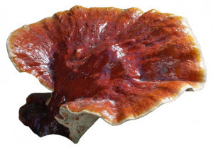
An Austrian research team is investigating the growth and processing of fungal mycelium skins as a biodegradable substrate material for sustainable electronics. The focus of their work is a fungus from the family of lacquered mushrooms - Ganoderma lucidum.
An Austrian research team is studying the growth and processing of fungal mycelial skins as a biodegradable substrate material for sustainable electronics. The focus of their work is a fungus from the Ganodermataceae family.
Polyester films or, for high demands, polyimide films are usually used as the base material for flexible printed circuit boards. These are further processed with the aid of the usual processes used in conventional PCB technology, such as chemical and galvanic copper deposition, photolithographic structuring and etching of the conductor tracks. Polyimide films are characterized, among other things, by their very high bending strength, high dielectric strength and high temperature resistance during soldering. Flexible printed circuit boards are used wherever the component carrier has to be bent many times during its service life or the assembly design requires the component carrier to be folded. This can be the case in portable electronics, medical technology or consumer electronics, for example.
Sustainability in the electronics industry requires the substitution of these non-degradable and difficult-to-recycle materials with materials that are either biodegradable or easy to recycle. An Austrian research team led by Doris Danninger from the Johannes Kepler University Linz is taking an unusual approach. They have developed a concept for the growth and processing of fungal mycelium skins as a biodegradable substrate material for sustainable electronics. After all, the base material is the second largest contributor to component mass after the circuitry, which has to be disposed of at the end of its service life.
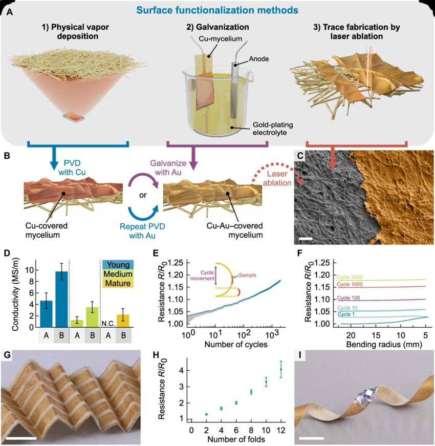
- Production options for structured mycelium skin
- Formation of Cu and Cu-Au bilayers on the mycelium skin
- Colorized SEM image of a laser ablated edge of a Cu-Au layer
- Conductivity of a PVD Cu-Au layer on young, medium and mature mycelium skin
- Normalized resistance of the young Cu-Au-covered mycelium during cyclic bending over 2000 times with bending radii from 5 to 25 mm
- Normalized resistance as a function of the bending radius
- Cu-Au traces on a young mycelium skin after folding
- Standardized resistance of the conductors increases with the number of folds
- Young mycelium skin with surface-mounted LED
Image: Johannes Kepler University Linz
By combining conventional (possibly reusable) ICs with a biodegradable substrate instead of polymers that are difficult to recycle, electronic waste could be significantly reduced. At the end of the PCB's life, reusable surface-mounted components can be easily removed from the board using simple tools such as a heat gun or soldering iron, leaving only the biodegradable substrate as a waste product.
The basis for the new substrate is a fungus, the shiny lacquer fungus, which grows on dead wood in nature. More precisely, only the pure mushroom mycelium is produced artificially, which has promising mechanical properties and is completely biodegradable. The mushroom material can be fitted with conventional circuit components.
Production of the novel base material, the mycelium skin
 Danninger's research team produces mycelial skins by growing the mycelium on moist beech wood chips at 25 °C and in a humid atmosphere. It is important that only a mycelium skin forms and that the formation of fruiting bodies is suppressed in order to obtain a smooth skin. This is achieved by minimizing exposure to light and maintaining a highCO2 content in the surrounding atmosphere. After harvesting, the wet skins are compressed from the living mycelium and dried. The researchers achieved a maximum of five subsequent harvests from one culture medium over a period of six weeks.
Construction of the conductive pathways
The entire surface of the mycelium substrate is metallized using physical vapour deposition (PVD) with a 400 nm thick copper layer. For better adhesion of the copper to the smooth mycelium skin, a chromium adhesion layer 3 nm thick is deposited beforehand. To improve the conductivity of the conductor tracks, an additional 50 nm thick gold layer is applied to the copper.
The physical vapor deposition takes place in a vacuum in order to ensure high purity of the deposited metal layers and thus low electrical resistance. The deposition rates were 0.02 nm/s for chromium, 0.3 nm/s for copper and 0.15 nm/s for gold.
Using a different technology, the entire surface of the copper-plated mycelium was electroplated with gold using PVD. This electroplating process, which is well established in PCB technology, is easily scalable.
The conductor tracks are then structured by selective laser ablation rather than by etching, as is common in PCB technology. The mycelium substrate is not damaged in the process.
Properties of the mycelium substrate
The substrate obtained in this way exhibited thermal stability up to 250 °C, meaning that printed circuit boards can also be soldered on this basis later on.
The researchers found that only young mycelium skin with its smooth surface is suitable as a substrate material. Conductor tracks produced on it can withstand high current densities of up to 333 A/mm2. In addition to the high conductivity of 9.75 ± 1.44 × 10⁴S/cm, the circuit carriers are very flexible.
With a bending radius of between 22.5 and 5 mm, 2000 bending cycles are possible with a low increase in resistance of 18.1 %. After this, the metal film tears over a large area with each cycle, which leads to a significant increase in resistance. The circuit carriers can also be folded several times. The standardized resistanceR/R0 increased to 4.07 ± 0.51 after folding 12 times. This means that even very complex electronic assemblies can be realized with flexible printed circuit boards produced in this way.
In addition to the production of flexible printed circuit boards, the research team has developed new types of batteries from the mushroom material, which consist mainly of degradable mycelium. Follow-up work will also investigate how the membrane formed from the mushroom skin can be specifically adapted to a particular application.


