
To produce three-dimensional, electrically functional parts, electrically conductive printed and assembled thermoplastic films are thermoformed into a three-dimensional shape and then back-injected. With conventional processes, the degree of forming achieved is limited due to the homogeneous heating of the surface and the unavoidable inhomogeneous expansion. The core task of the project was to develop methods for the targeted control of the forming process, including selective heating and adjustment of the elongation.
For the production of three-dimensional electrically functional parts, electrically conductive printed and equipped thermoplastic films are formed into three-dimensional shapes by thermoforming processes and then back-injected. With conventional processes, the degree of forming achieved is limited due to homogeneous heating over a wide area and unavoidable inhomogeneous elongation. The core task of the project was the development of methods for the targeted control of the forming process including selective heating and adjustment of the elongation.
1 Introduction
The terms in-mold, conformable or structural electronics refer to the integration of electronic components and functionalities into freely moldable 3D surfaces for the development of innovative components and products [1-3]. The intended target markets include, for example, automotive and aviation, but also robotics, home and medical technology, printed circuit boards and packaging. For example, visionary interior, operating or component concepts based on interactive, smart and lightweight user interfaces with high demands on ergonomics, appearance and design are conceivable. The key technologies in focus here are based on printing and PCB processes which, in combination with the thermoforming and injection molding technologies typical for plastics, lead to completely new, hybrid manufacturing concepts and 3D surfaces and products. This clearly sets the technology apart from conventional 2.5 and 3D processes based on 3D embedding [4, 5], flex, rigid-flex [6] or 3D-MID [7]. The process sequence is shown in Figure 1.
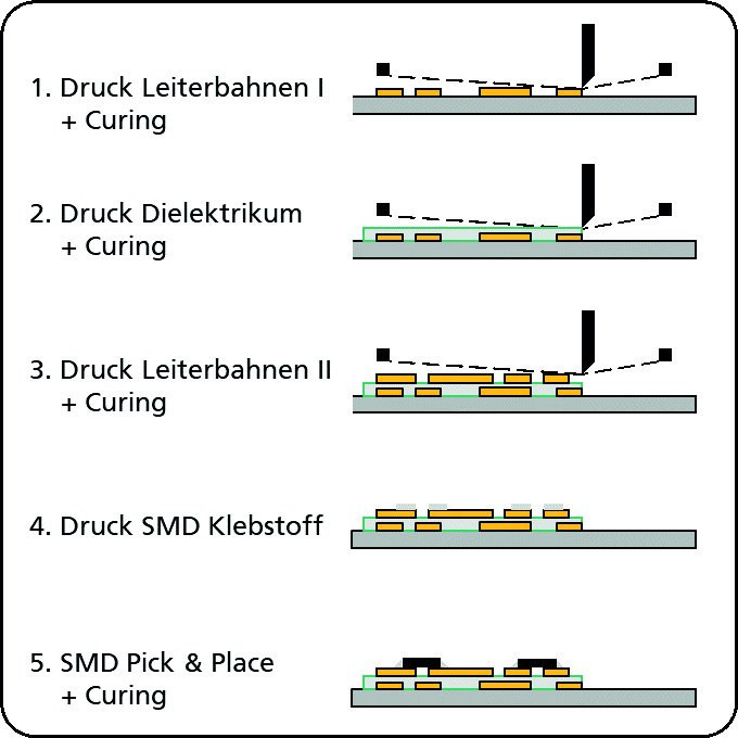
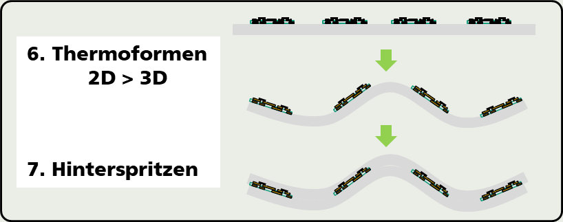
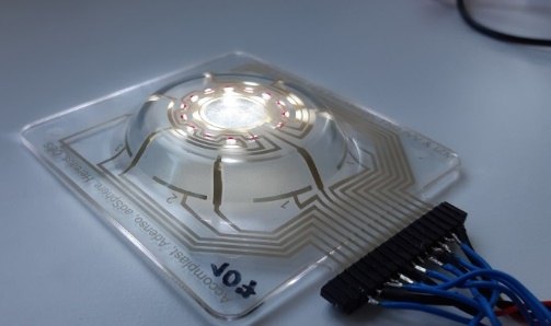
Fig. 1: Process sequence, demonstrator
Despite promising R&D results and recognizable commercial approaches, there is still a considerable need for research into the central issues: What thermoformability or stretchability do printed electrical conductors have? How can this be characterized under processing-relevant conditions? Which rules need to be taken into account in product design and which processes and technologies are suitable for precisely controlling the forming of the thermoplastic, structured and assembled semi-finished product? Furthermore, the overmouldability of printed, assembled and formed films as well as the resilience and reliability of corresponding modules are the focus of the investigation. This is where the Origami F2E (Free Form Electronics) project comes in, with the industrial partners Adenso (plant engineering), Accomplast (injection molded parts), Heraeus (conductive transparent inks), TES Frontdesign (operating and input systems, printing technology) and also plant engineering and demonstrator development representing important work packages. The composition of the consortium, including the participating research institutes (FhG-IVV, FhG-IZM) and two other associated project partners (Fujikua Kasei, JSW/Japan), thus covered all the sub-processes required for the process chain, including printing materials, necessary preliminary tests, simulations, reliability tests and analytics.
2 Material and component selection, demonstrator concept
When selecting materials, the focus was on (partner) compatibility and a large overlap with all sub-processes. In terms of film technology, basic tests, in particular thermoforming tests, were carried out on PC (polycarbonate), PET (polyethylene terephthalate), PMMA (polymethyl methacrylate) and PVC (polyvinyl chloride). PC proved to be the material favored for the duration of the project, with the best properties in terms of printing, thermoforming and back-injection. The selection of printing pastes was based on electrically conductive, electrically non-conductive or insulating, electrically conductive and transparent pastes as well as decorative inks. The focus was on the use of materials from Heraeus GmbH (Pedot Clevios, transparent, electrically conductive) and from the associated Japanese partner Fujikura Kasei (electrically conductive, insulating). As a benchmark, materials, i.e. conductive pastes, from other manufacturers (Namics, DuPont) were also examined. Colors from Pröll were examined for decorative purposes.
The selection of components was essentially based on the demonstrator concept developed and included SMD LEDs and resistors of sizes 0201, 0402, 0603, 1206 as well as VSOP8 housings (resistor array) representative of active components.
This made it possible to examine the overmouldability of various pastes (Ag conductive paste, protective lacquer, Pedot Heraeus-Clevios) as well as component compatibility and developed assembly and connection technology. The test samples were also used for reliability tests.
The interactive demonstrator consisted of a 3D surface (shell 10x10 cm2) in the form of a knob or rotary control, with strong forming in the knob area and LED lighting controlled by touch functionality, with all components fully embedded and overmolded. Components and functionalities (LEDs, touch pad) are placed in the molded central area, which, thanks to temperature profiling, is hardly heated and deformed(Fig. 2).
 Design") a) Design
a) Design
 Test gedruckt/umgeformt") b) Printed/formed test
b) Printed/formed test
 Demonstrator") c) Demonstrator
c) Demonstrator
Fig. 2: Demonstrator, design and prototypes
The chosen concept proved to be a good compromise between versatile functional integration, with the potential for step-by-step design adjustments and an increase in complexity, and cross-partner compatibility in terms of size, format and functionalization.
3 Heating and forming process
After comparing different heating methods, a combined two-stage heating process was developed for the forming of the hybrid material (carrier substrate with printing / assembly). A pixelated contact heater is used to apply temperature profiles so that the temperature level can then be increased to the required forming temperature using a radiator. Based on the applied temperature profile, the elongation behavior can be specifically controlled depending on the forming [8]. Exclusive processing using contact heaters is not possible due to the heating behavior of the substrate material used. From a temperature > 150 °C, there were adhesion effects between the contact heater and the carrier substrate used. As a result, the surface of the hybrid material was damaged.
Numerical and experimental simulation were combined to develop application-specific temperature profiles. The numerical simulation is used to map the forming behavior(Fig. 4) [9]. For example, local strain maxima (equivalent stress hypothesis) can be determined as a function of the process variables. The heating and cooling behavior(Fig. 3) and material-specific properties (reflection, transmission, absorption) were taken into account for the comparison of the heaters used.
 Fig. 3: Resulting temperature distribution - from left to right: targeted temperature profiling; inhomogeneous temperature profile due to adhesion effects; homogeneous heating using radiators; homogeneous heating using radiators, cooling behavior after 10s
 Fig. 4: Simulation model of formingTheprocess behavior of the conductor tracks was quantified by means of experimental simulation. Changes in resistance as a function of the process variables and as a result of the strains can thus be determined. For the design of the main system-related tests (thermoforming tests), initial investigations into the ductility of conductive pastes were carried out using uniaxial tensile/strain tests in a heated chamber and online measurements. Using four-point measurement and a data logger, the electrical resistance and the functionality of the structures could be recorded online, i.e. during the stretching process. In summary, the following could be determined:
- the percentage resistance curve is almost independent of the conductor track width (see also the result of the thermoforming test(Fig. 7)).
- in general, the elongation and resistance behavior is strongly dependent on the initial or curing state of the print pastes as well as the temperature input during the tests
- Due to the relatively slow convective temperature input (oven), slow deformation speeds and only uniaxial stretching compared to thermoforming (radiator), the results are only transferable to a limited extent.
Uniaxial tensile tests on printed conductors with a meandering pattern(Fig. 5a) did not show any recognizable increase in ductility compared to straight conductors. With homogeneous elongation over the entire surface, in close contact with the film, the structures exhibit approximately the same, and in some cases lower, elongation properties than straight conductors(Fig. 5). An effect similar to that of photolithographically produced Cu tracks [1, 2]) with the ability to transfer tensile stresses and corresponding track deformation is not recognizable(Fig. 5d).
 Fig. 5: Extensibility of meandering conductors
The results of the uniaxial tensile tests were used for the design of the thermoforming tests, which were realized according to the principle of statistical test planning.
A test arrangement based on the principle of space filling was used so that the test environment could be easily expanded. The test design used for the test samples is divided into test sections. The measured resistance value of the individual sections before and after forming acted as the target variable. The influencing variables in this application are the heating temperature and time, the forming pressure, the width of the conductor tracks and the local stretching. A total of 1188 test points were examined for the development of the regression model, of which 1137 were used to calculate the model. The results of the analysis are listed below:
- Accuracy of the model is 94.2 %
- The main effect or main influencing variable on the target variable is the distortion
- Logarithmization of the target variable is mandatory
- all interactions of the influencing variables are relevant for determining the target variable
- a maximum elongation of 84 % can be achieved
- with increasing forming pressure and heating times, the maximum achievable stretching deteriorates.
Using regression, it is possible to determine the expected resistance value and the maximum possible stretching depending on the forming parameters used. In combination with the numerical simulation, it is thus possible, for example, to test and optimize PCB layouts with and without components with regard to their suitability for thermoforming. It is also possible to determine the optimum process conditions (e.g. temperature profile, heating times, forming pressure) for an existing layout or molded part. Figures6 to 8 show the interdependencies.
 1 Test design
 2 Arrangement of the test points
Fig. 6: DoE - SpaceFilling
 in Abhängigkeit der Einstellgrößen (SI) am Beispiel eines Versuchspunktes") Fig. 7: Change in resistance values (Ohm) as a function of the setting variables (SI) using the example of a test point
Fig. 7: Change in resistance values (Ohm) as a function of the setting variables (SI) using the example of a test point
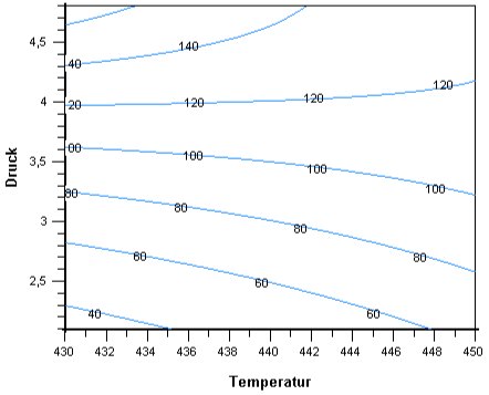
Fig. 8: Contour diagram of the change in resistance using the example of the emitter temperature, heating time and pressure (SI) with a stretching of 65 %
4 'InMold Electronics' and reliability
The overmoldability of pre-structured assembled films was investigated analytically and experimentally. The main aim was to understand the stability (and functionality) of printed structures and bonded SMD components during the injection process under high temperature, speed and pressure of the melt. Numerical simulations were carried out by JSW (Japanese manufacturer of injection molding systems) in comparison with the evaluation of assembled and overmolded 2D test samples (test plate, Fig. 9.5 and 9.6). This allowed initial estimates to be made of the maximum adhesive and shear strengths of printed layers and assembled components (connection quality). In addition, this makes it possible to design any 3D geometries with regard to permissible injection molding parameters (pressure, temperature, speed) and to draw conclusions about critical or permissible component positions and tool design (e.g. sprue position).
For example, different paste types show different stability and adhesion depending on their microstructure, irrespective of possible substrate pre-treatments, whereby it became clear, for example, that partially sintered or cross-linking Ag nano structures also exhibit high stability in areas close to the gate, i.e. highly stressed areas(Fig. 9.1-9.4). With regard to the shear strength of bonded components, however, these zones prove to be critical and can only be overmolded without damage at very low flow rates, for example(Fig. 9 5.-9.6.).
 Fig. 9: Adhesion of print pastes of different types near the gate and corresponding micro-nanostructures; overmolded test panel > sheared components
Based on these preliminary tests, to produce overmolded samples primarily for reliability tests (accelerated aging under different climatic conditions), two versatile 2D test designs were developed(Fig. 10).
 Teststruktur A inkl. Pedot Clevios transp") a) Test structure A incl. Pedot Clevios transp
a) Test structure A incl. Pedot Clevios transp
 Teststruktur B") b) Test structure B
b) Test structure B
Fig. 10: Functional, PC encapsulated 2D test structures
The conductor and electrode structures are based on printed Ag and Pedot bases (transparent, Heraeus), fitted with SMD LEDs and 0 Ohm resistors of sizes 0201, 0402, 0603, 1206 as well as VSOP8 housings (resistor array) representative of active components. For electrical measurements and contacting, conductor paths lead from the single-layer printed and back-molded composite into peripheral, non-back-molded film areas. The objective achieved was the development of a high-throughput, fully inline-capable assembly process, including conductor track and adhesive printing, dispensing of adhesive (non-conductive), assembly and necessary curing steps up to the minimum component size 0201 and minimum contact spacing of 325 µm (650 µm pitch). Due to the structuring of non-solderable surfaces and the limited temperature stability of the films, the focus was on adhesive technologies. In addition to the printed depots for electrical contacting, strength-enhancing dispense adhesive dots proved to be essential for achieving the necessary stability in the subsequent processes, particularly with regard to injection molding.
The following results were obtained after overmolding:
- Test structure A: 100% component and module yield after overmolding (1407 components in total, 21 boards)
- Test structure B: 97.9 % component yield, 50 % module yield after overmolding (a total of 2736 components, 24 boards)
- overmolded Pedot structures show a layer thickness-dependent 20 % (screen A) or approx. 8 % (with screen B > finer mesh) increase in resistance values after overmolding
- when using a protective coating, the web resistances remain almost unchanged
- printed conductive structures based on Ag paste show a reduction in web resistance (approx. 20 %) after overmolding.
The test conditions for reliability tests were selected based on automotive standards in the interior area. In summary, the following results were obtained:
- Thermal ageing at 70 °C / 336 h (2 weeks) under load (LED rated operation)
- All LEDs functional at the end of the test (4 boards in total)
- Pedot structures show no significant resistance changes
- Thermal shock load at -40 / + 80 °C, 20 min. soaktime, for 500 cycles
- All LEDs functional at the end of the test (6 boards in total)
- Pedot structures show no significant resistance changes
- printed Ag structures show no significant changes in resistance values
- all other SMD components show unchanged functionality or intact contacting after the end of the test without significant change in the test contact resistances
- Temperature-humidity exposure at +40 °C / 93 % RH for 336 h (2 weeks)
- All LEDs functional after end of test (6 boards in total)
- Pedot structures exhibit coating-independent resistance changes in the sense of decreasing resistance values after the end of the test (10-20 %).
A detailed analysis was carried out, which included an electrical, optical and microscopic examination of cross-sections. The optical and microscopic analysis resulted in a relatively unremarkable and uncritical (fault) picture overall, which is also consistent with the electrical functionality determined after the test (no failure). In summary, the following results were obtained:
- no test-specific abnormalities due to the effects of temperature or humidity were detected
- the selected SMD test components of different types (1206, 0603, 0402, 0201, VSOP8 > R, LED) are basically suitable for back-molding
- One aspect made clear by the cross-section analysis is the occasionally visible deformation of components as a result of the injection pressure depending on the component type and assembly technology. Here it becomes clear that it is sometimes necessary to support components by underfilling them with adhesive or to select components accordingly
- Only in isolated cases, especially with ceramic-based components with a larger design (resistors from 1206), do component fractures occur, mostly due to a lack of the above-mentioned underfilling, caused by isolated process errors during assembly or dispensing
Figure 11 shows an excerpt of the results with the occasional defect patterns and anomalies.
|
Initial, top view |
LED 0603 |
|
 |
 |
|
|
Initial, cross-section |
LED 0603 |
|
 |
 |
|
|
TWT -40/+80 °C / 500 cy., |
||
|
LED 0201 |
LED 0402 |
LED 0603 |
 |
||
|
||
|
0 Ohm 0603 |
0 Ohm 1206 |
0 Ohm 1206 |
|
o. k. |
o. k. |
Component breakage |
5 The demonstrator
The demonstrator has been realized in multiple versions with the cooperation of all project partners. To test the functionality and for demonstration purposes, control circuits based on microcontrollers were developed, which demonstrate the possible basic functions depending on the configuration(Fig. 12).
Using microcontrollers (Arduino) and an additional IC or evaluation board for capacitive evaluation(Fig. 12), touch-dependent LED functionalities were realized, with
- V1: On/off control via central, transparent pedotouch surface; selection of LED ring I/II, control of brightness, flashing frequency, strobe-flash on/off via the seven lateral pedotouch surfaces
- V2: Control on/off via central transparent Pedot surface; selection of LED ring I/II + dimming by slider function via the seven lateral touch surfaces.
 V1 mit Touch-Funktion") a) V1 with touch function
a) V1 with touch function
 V2 mit touch-slide Funktion") b) V2 with touch-slide function
b) V2 with touch-slide functionFig. 12: Interactive project demonstrator; touch-controlled LED activity
6 Summary
The research project on innovations with organic electronics (Origami) and the sub-project 'Investigation and development of moldable printed components (F2E / Free Form Electronics)' as well as the resulting findings have highlighted the great potential of thermoforming processes based on time- and location-resolved substrate heating. The demonstrator applications have shown that the technology leads to greater design freedom in terms of shape, location and positioning of electronic components and greatly increases the variety of possible applications. The characterization, in particular of the strain-dependent electrical conductivity, of different substrate and print paste materials using various, sometimes complementary methods, has led to a comprehensive understanding of materials and processes. Demonstrator and test designs have shown that the development of an assembly and connection technology compatible with thermoforming and injection molding, based on electrically conductive adhesives and conventional SMD assembly processes, is possible. Reliability tests based on automotive standards (interior) have shown that the basic requirements for use, in terms of electrical functionality and service life, can be met. An evaluation of other criteria such as surface or color quality was not the subject of this study.
Acknowledgements
The project 'Innovations with organic 3D electronics', sub-project 1: 'Investigation and development of formable printed components' (VKN 03INT509B) presented here in excerpts was funded as part of the internationalization of clusters of excellence, future projects and comparable networks of the Federal Ministry of Education and Research, carried out in cooperation with the partner cluster Yonezawa (Japan) and coordinated by Organic Electronics Saxony e. V. (OES).
Literature and references
[1] Kallmayer, Ch.; Löher, T.: Conformable Electronics - formbare Elektronik, In: PLUS, Produktion von Leiterplatten und Systemen Vol. 19 (2017), No. 4, pp. 728-732.
[2] Löher, T.; Seckel, M.; Haberland, J.; Marques, J.; v. Krshiwoblozki, M.; Kallmayer, Ch.; Ostmann, A: Conformable Electronics: Integration of electronic functions into static and dynamic free form surfaces, IEEE CPMT Symposium Japan, ICSJ 2019, Nov. 18 - 20, 2019, Kyoto, Japan
[3] Simula, T.; Niskala, P.; Heikkinen, M.; Rusanen, O.: Component Packages for IMSETM (Injection Molded Structural Electronics), 2018 IEEE, Published at NordPac, 2018 Annual Conference. June-12-14, Oulu, Finland
[4] Ostmann, A.; Neumann, A.; Sommer, P.; Reichl, H.: Buried components in printed circuit boards, In: Advancing Microelectronics (2005)
[5] Boettcher, L.; Manessis, D.; Ostmann, A.; Karaskiewitz, S.; Reichl, H.: Embedded Chip Packages - Technology and Applications, p. 6
[6] Rigid-flex printed circuit boards - CONTAG AG, URL http://www.contag.de/leiterplatten.php?leiterplatten_produkte_starrflex.html.- retrieved on 2019-03-27
[7] Zhuo, Y.; Alvarez, Ch.; Feldmann, K.: An integrated design system for molded interconnect devices (3D-MID)
[8] Martens, J.: Profiling of the semifinished product temperature to increase the material efficiency during thermoforming, Dissertation, Verlagsgruppe Mainz GmbH, 2018
[9] Sanjon, C.: Material characterization of plastics for thermoforming using new measurement technologies, VVD, Dresden, 2018
Image references
Unless otherwise stated, the image rights are held by Fraunhofer IZM and Fraunhofer IVV.
Fig. 2b, 2c: adSphere, www.adsphere.solutions
Introductory image: Courtesy of InfraTec Gmbh Infrarotsensorik und Messtechnik, www.infratec.de
