Researchers at the Fraunhofer Institute for Reliability and Microintegration in Berlin have developed an integration technology to protect sensitive electronic components from environmental influences with a biocompatible and soft encapsulation. In the ECSEL project 'APPLAUSE', funded by the European Commission, one of the goals was to develop a flexible and stretchable patch to measure the vital functions of heart patients.
Researchers at the Fraunhofer Institute for Reliability and Microintegration in Berlin (IZM) have developed an integration technology to protect sensitive electronic components from environmental influences with a biocompatible and soft encapsulation. In the ECSEL project 'APPLAUSE', funded by the European Commission, one of the goals was to develop a flexible and stretchable patch to measure the vital functions of heart patients.
The overarching aim of the 'APPLAUSE' project was to develop cost-effective manufacturing and integration technologies for microelectronics - especially optoelectronics - in Europe. The developed patch system includes LEDs, system-on-chips, flash memory and acceleration sensors. The data recorded and processed in the system enables cardiological monitoring by means of a photoplethysmogram (PPG) as well as monitoring of oxygen saturation (SpO2), respiratory movement and bioimpedance. In addition to system and circuit development, the researchers at Fraunhofer IZM focused on assembly and connection technology and the integration of a densely packed flexible circuit carrier into the patch. To this end, a process was developed that combines thin-film technologies with stretchable substrates in order to realize complex systems for applications close to the body.
Technology and parameter determination
 Fig. 2: Process sequence for thin-film flex integration into the TPU substrateThermoplasticpolyurethane (TPU) was usedas thecarrier film for the plaster, as its flexibility and elasticity make it very comfortable to wear on the body. Furthermore, the material can be processed cost-effectively and industrially using printed circuit board technologies (the production format used was 610 mm x 457 mm).
First, it was shown that very thin and densely wired complex flex circuits can be integrated and electrically connected in a TPU structure. The thin-film flex circuit based on polyimide with dimensions of 12 mm x 9 mm had a total thickness of 50 µm, contained two 20 µm thick test chips (with daisy-chain structures and copper contacts) as embedded components and was developed and provided by the Wafer-Level System Integration department at Fraunhofer IZM (Kai Zoschke). The test setup was used to investigate the maximum possible wiring density inside the PI-Flex and the connection density to the TPU substrate. The arrangement in daisy-chain format made it possible to examine and test the entire system via the fan-out structures in the TPU part, including the structures of the embedded PI-Flex inside.
Before embedding the PI-Flex, transparent TPU films were first cut to size using a UV laser. The individual TPU films, the flex circuit and a 5 µm thin Cu film were mechanically aligned to each other in a stable manner using pinning. The subsequent lamination was carried out in a short-cycle press at 165 °C and a pressure of 10 bar (see Fig. 2). Thanks to previously implemented recognition marks in the layout, µ-vias (diameter 90 µm) could then be placed to contact the fan-out structures in the TPU and the contact pads in the PI-Flex using a UV laser. The challenge here was to find suitable parameters to expose the copper surface of the contacts, drill approx. 50 µm deep through the TPU and stop on the copper pads of the flex circuit, which are only 10 µm thin.
The electrical contact was made by electroplating copper into the µ-vias. Traces and measuring contacts were defined in the final step using photolithography and etching.(Fig. 3).
 Fig. 3: Blind vias from the TPU substrate to the PI-Flex. On the right is the test chip with DC structures
 mit eingebettetem PI-Flex (mittig) und Testlayout") Fig. 4: TPU substrate (total thickness 150 μm) with embedded PI-Flex (center) and test layout
Fig. 4: TPU substrate (total thickness 150 μm) with embedded PI-Flex (center) and test layout
 Fig. 5: Adapted process sequence with different componentsThesubstrates were characterized during the entire process chain by means of optical and electrical measurements. The process parameters for lamination were optimized so that none of the embedded Si chips exhibited fractures in the optical inspection. The electrical testing of twelve structures showed low contact resistance and completely continuous daisy chains. The overall result was that all structures were contacted, i.e. all microvias between the TPU substrate and the PI thin-film flex were functional. Electrical measurements carried out after final reliability tests (200 h at 85 °C and 85 % humidity) showed that there were no significant deviations from the initial measured values.
Structure of the TPU module
A functional system was created based on the results of the development phase. This means that a measurement and evaluation module, which was manufactured using thin-film flex technology, was encapsulated in TPU to protect it from mechanical and environmental influences. The functional circuit carrier consisted of a three-layer polyimide thin-film flex with a thickness of 50 µm. The components used were more varied and in greater numbers than in the test setup, but also had considerable differences in height, ranging from 50 µm (ICs) to 1 mm (commercially available SMD components). It was therefore necessary to adjust some process parameters. For lamination in particular, several individually cut TPU foils were used in the press stack to compensate for the height differences and to ensure a uniform material flow of the TPU during the melting process. As the measuring module had several signal outputs, another challenge was to place the microvias precisely on the contacts.
As the module was to be soldered onto the actual patch substrate, the contacts leading to the outside were silver-plated in a wet-chemical bath. After completion of the processes, the module was separated by laser according to the contour.
 mit unterschiedlichen Bauelementen") Fig. 6: Three-layer PI-Flex (50 μm thin) with different components
Fig. 6: Three-layer PI-Flex (50 μm thin) with different components
 Fig. 7: Individual TPU foils for height compensation
 mit den Maßen 25 mm x 18 mm x 1,2 mm") Fig. 8: Complete TPU module (SiP) with the dimensions 25 mm x 18 mm x 1.2 mm
Fig. 8: Complete TPU module (SiP) with the dimensions 25 mm x 18 mm x 1.2 mm
TPU paving structure and installation
For the development of the integration into the patch, a test layout was developed to examine the soldering of the TPU module and other SMD components. The layout contains copper electrodes (without silver chloride coating) and has partially meandered conductor tracks to ensure the stretchability of the conductor tracks under tensile stress. The same 100 µm TPU film was used to produce the carrier film for the patch demonstrator as for the test module described above. The single-layer wiring layer consisted of 5 µm thick copper. However, unlike conventional PCBs, the solder resist was only applied locally around the contact surfaces so that the flexible/elastic character of the polyurethane film was retained on the surface of the patch. The copper structures were then silver-plated with no current, fitted with the test components (SMD, TPU module and switch) and soldered in a reflow oven at 162 °C using SnBi solder. Finally, the demonstrators were separated using a laser.
 Fig. 9: Selective solder resist on patch demonstrator
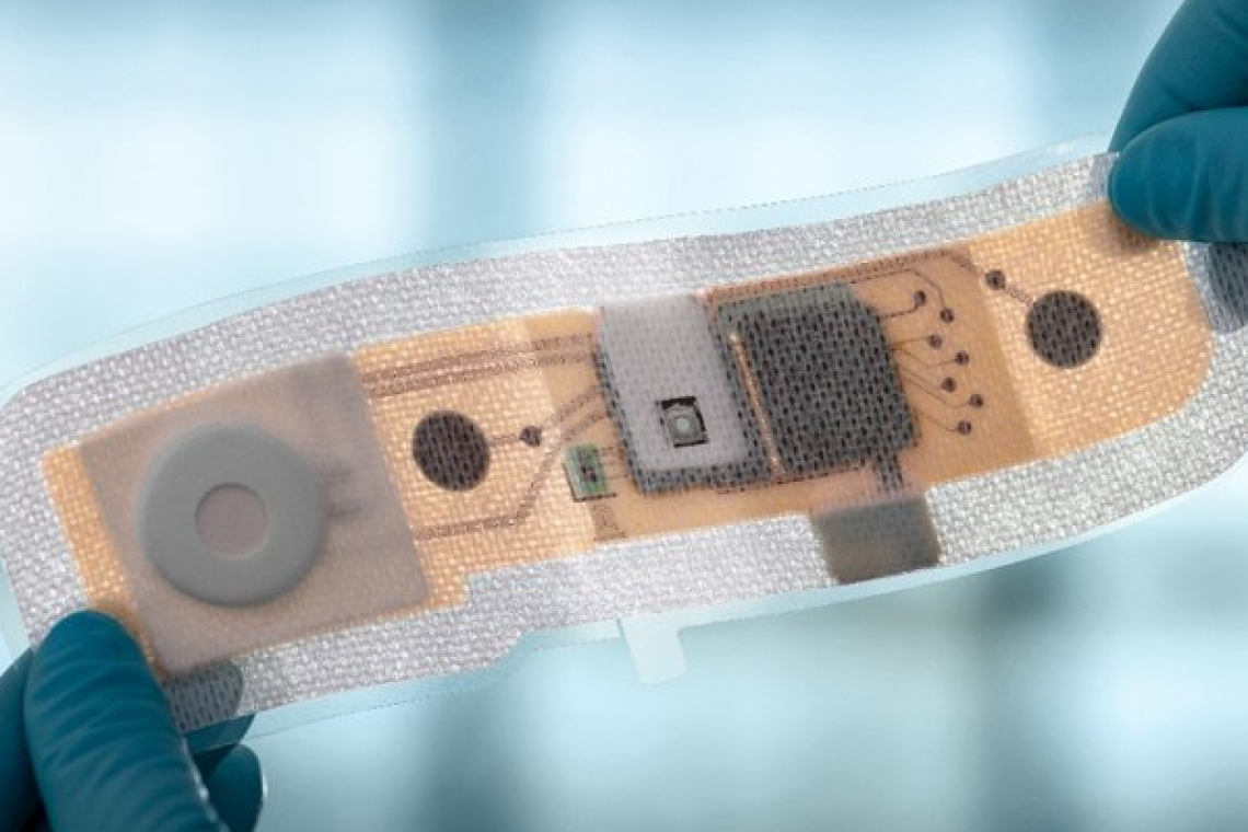
 Fig. 10: Patch demonstrator with soldered TPU module and SMD components
Conclusion
It has been successfully demonstrated that robust and reliable TPU encapsulation of thin (polyimide) circuit carriers is possible. The TPU embedding of ultra-thin chips integrated in polyimide and surface-mounted SMD components can be realized using standard PCB processes. The functionality of the circuit is not impaired by the processing or the material and the encapsulation provides the components with the necessary protection against environmental and stress influences resulting from the application scenario. The TPU package can be soldered to circuit carriers using SnBi solder. Alternatively, electrically conductive bonding would also be possible with generously dimensioned copper structures and spacings. For the application, the patch is also provided with printed electrode surfaces and skin-friendly adhesive films to increase wearing comfort. A two-layer TPU substrate (with vias) would also be conceivable if the circuit design requires this or to increase the packing density. A textile surface, which could be laminated onto the TPU film of the patch in advance, could be conceivable as a further optimization.
Image sources
Fraunhofer IZM
References
[1] L. Boettcher; D. Manessis; A. Ostmann; S. Karaszkiewicz; H. Reichl: Embedding of Chips for System in Package realization - Technology and Applications, 2008 3rd International Microsystems, Packaging, Assembly & Circuits Technology Conference, 2008, 383-386, doi: 10.1109/IMPACT.2008.4783892
[2] N. Islam; K.H. Tan; S.W. Yoon; T. Chen: High Density Ultra-Thin Organic Substrates for Advanced Flip Chip Packages, 69th Electronic Components & Technology Conference, Las Vegas, USA, May 28th-May 31st, 2019
[3] J.P.L. Leenen; C. Leerentveld; J.D. van Dijk; H.L. van Westreenen; L. Schoonhoven; G.A. Patijn: Current Evidence for Continuous Vital Signs Monitoring by Wearable Wireless Devices in Hospitalized Adults: Systematic Review, Journal of Medical Internet Research, 2020 Jun 17;22(6): e18636, doi: 10.2196/18636, PMID: 32469323; PMCID: PMC7351263
