The article summarizes experiences on convection types and the resulting interactions on planar surfaces, discusses the background and presents possible solutions. The aim is to illustrate the processes at the heterogeneous interface during wet chemical treatment. In addition, a method will be presented with which the local current distribution during galvanic deposition can be determined directly on a PCB panel. The method can be used to determine local influences without interference. Process settings can also be optimized under real conditions.
This article summarizes experiences with convection types and the resulting interactions on planar surfaces, discusses the background and presents possible solutions. The aim is to illustrate the processes at the heterogeneous interface during wet-chemical treatment. In addition, a method is presented with which the local current distribution during galvanic deposition can be determined directly on a conductor plate panel. With this method, local influences can be determined without interference and the process settings can be optimized under real conditions.
The wet chemical treatment of surfaces is essential for the construction of circuit carriers. It is used in particular in the deposition and etching of copper for PCB production and in surface finishing in various process steps. A particular challenge of the present and future in this context is the growing demand for structure accuracy in three dimensions (layer thicknesses, vias, structure widths and distances) with the largest possible processing format. In order to meet these requirements, deposition and etching processes must be carried out with maximum uniformity over the entire panel surface.
Convection is a key factor influencing the treatment result in such processes. For this reason, considerable technical effort is put into generating suitable convection (sample movement, gas introduction, flow). Nevertheless, most technical solutions are based more on experience and tradition than on calculations by designers.
With the method presented here, local influences can be determined without interference and the process settings can be optimized under real conditions.
1 Convection at heterogeneous interfaces
In the production of circuit carriers, the main processes for building up and structuring the metallization take place using aqueous solutions. The reaction zone is always the transition area from the liquid to the solid phase. This is where the reactants from the solution are brought to the interface in order to deposit material in a chemical reaction (e.g. deposition of a surface finish) or to dissolve material (e.g. etching of conductor structures). The state of this heterogeneous interface between the solid and liquid phases is decisive for the quality of the chemical processes in relation to the overall surfaces (circuit carrier format). The structure of the transition area is described in Figure 1.
 Fig.1 : Schematic representation of an interfacial reaction using the example of metal deposition
It can be seen that the transport of the reactants to the interface must take place through different zones. In the electrolyte volume, the transport or concentration equalization is initially determined by convection. Directly at the surface there is a directed arrangement of ions and charge carriers, known as the Helmholtz double layer. This is followed by a relatively thin area that is also not covered by convection. In this so-called diffusion layer, mass transport takes place exclusively through concentration equalization. The thickness of the diffusion layer can vary greatly and is a limiting factor for the reaction rate.
Using galvanic deposition as an example, the processes involved in cathodic deposition can be described as follows:
- Free or field-supported movement of the metal ions in the convection space
- Diffusion of the metal ions to the cathode surface,
- stripping of the hydrate shell,
- Passage through the Helmholtz charge zone,
- Reduction of the metal ions,
- crystallization.
An etching process can be described as follows:
- Diffusion of oxidizing agent and auxiliary substances to the surface,
- stripping of the hydrate shell,
- Passage through the Helmholtz charge zone,
- Redox reaction at the heterogeneous interface,
- Hydration or complexation of the metal ions and passage through the Helmholtz charge zone,
- Diffusion of the reaction products into the solution volume.
The overall speed and thus also the maximum achievable deposition speed are determined by the slowest partial step. In electroplating (but also in equilibrium reactions at heterogeneous interfaces), diffusion is of decisive importance here. In the area close to the surface (up to approx. 100 µm), the mass transfer of the reaction partners essentially takes place by concentration equalization, i.e. diffusion. The concentration gradient is caused by the reaction on the surface and in the quasi-stationary state depends on the reaction speed or current density, the diffusion coefficient, the electrolyte concentration and the diffusion layer thickness. With the aid of Fick's 1st law and Faraday's 1st law, the so-called diffusion limit current, i.e. the current density at which the ion concentration of the deposition metal at the phase boundary approaches zero, can be calculated (equation (1)). The maximum reaction rate is reached in this state.

If the Einstein-Stokes equation (2) is applied to the diffusion coefficient, it can be seen that the limiting current density or maximum reaction rate is directly or reciprocally proportional to the temperature, the metal ion concentration, the viscosity of the solution, the ionic radius and the diffusion layer thickness (see Eq. (3)). It can be assumed that temperature, pH and composition are largely optimized in aqueous electrolytes and offer little scope for increasing reaction rates.
In contrast to these parameters, forced convection offers significantly greater scope.
|
Flow conditions |
δ [µm] |
ig [A/dm²] |
Remarks |
|
Natural convection in heated electrolyte |
150 - 200 |
1,44 |
Vertical electrodes |
|
Air introduction (0.1 l/min) |
100 |
2,76 |
Inflow through frit |
|
Laminar flow (25 cm/s) |
100 |
3 |
|
|
turbulent flow [94 cm/s) |
~ 40 |
8,1 |
Surge flow |
|
turbulent flow (25000 cm/s) |
~10 |
365 |
Jet flow |
As demonstrated in [1] using the example of sulphuric acid copper electrolytes, the limiting current density can be increased by a factor of 100 or more by optimizing convection conditions and thus reducing the diffusion layer thickness (see Table 1). The most effective effects were achieved with a strong turbulent flow over nozzles. The schematic representation of the incident flow when using nozzles (see Fig. 2, [2]) illustrates the fundamental difficulties in achieving homogeneous incident flow in the transition region from the ramjet to the deflection jet.
It is therefore clear that forced convection is absolutely necessary to achieve the shortest possible reaction and process times. However, in order to achieve a homogeneous reaction behavior over the entire reaction surface (panel format), the real challenge is to design the convection evenly over the panel surface. As the interactions between direct upstream flow and laminar downstream flow could not be controlled with conventional systems, turbulent flow systems according to Table 1 have not been used up to now, at least in PCB electroplating.
Of course, the relationship between convection and concentration gradients does not only apply to planar surfaces, which was impressively demonstrated in a simulation by [3](Fig. 3).
 Fig. 2: Jet propagation with incident flow on planar surfaces via nozzles [2]
![Abb. 3: Parameterstudie zur Anströmung eines Formteils und resultierenden Konzentrationsgradienten in der Galvanik [3]](/images/stories/Abo-2024-01/plus-2024-01-077.jpg "Abb. 3: Parameterstudie zur Anströmung eines Formteils und resultierenden Konzentrationsgradienten in der Galvanik [3]") Fig. 3: Parameter study on the flow onto a molded part and resulting concentration gradients in electroplating [3]
Fig. 3: Parameter study on the flow onto a molded part and resulting concentration gradients in electroplating [3]
The distribution of the electric field is also important in electroplating deposition systems. It can also lead to an uneven distribution of local current densities (e.g. between the edge and center areas of a panel) and therefore has a significant influence on local reaction rates and concentration gradients through the diffusion layer.
2 Optimized convection systems for electroplating
While chemical etching for structuring circuit carriers is predominantly based on spray etching systems in horizontal flow and these systems are considered to be sufficiently reliable in terms of etch rate homogeneity with few limitations, there are different concepts and solutions for electroplating, including for electronic components (e.g. lead frame strip electroplating, vertical panel plating, wafer fountain plater). What these systems have in common is the parallel plate arrangement, which is important for field distribution. Convection is realized in the techniques mentioned by circulation, fabric movement, air introduction or spraying systems in various combinations. Two recent developments for optimizing the flow problem will be presented here.
2.1 Gravity-assisted convection
Gravity-assisted electroplating takes place without forced convection in a horizontal parallel plate arrangement in which the cathode is positioned at the bottom(Fig. 4). As a result, the electrolyte density is reduced above the cathode surface due to the metal concentration gradient and density gradient-driven convection sets in, which is similar in principle to a Benard cell [4] with the difference that the density gradient is generated by temperature differences. Due to the lack of forced convection, only very low current densities can be realized. The advantage is the absolute homogeneity of the electrolyte movement, which also essentially only takes place in the active deposition areas. The process is used to deposit gold crystallites with a broad base and preferential orientation in the electrolyte volume as a functional surface for various applications [5] [6]. Characteristic deposition structures are shown in Figure 5.
, schwenkbare 8″-Waferzelle (rechts)") Fig. 4: Electrode arrangement in gravity-assisted electroplating (G-plating, left), pivoting 8″ wafer cell (right)
Fig. 4: Electrode arrangement in gravity-assisted electroplating (G-plating, left), pivoting 8″ wafer cell (right)
 Fig. 5: G-plating structures of gold bumps on an 8″ wafer
2.2 Direct current system with electrolyte recirculation
The direct flow principle described in [7] includes, among other things, the separation of the flow and return flow areas, which enables the avoidance of laminar-dominated return flows and thus significantly higher flow rates and subsequently higher reaction rates through suitable nozzle arrangements. The system can be realized as a 2-chamber nozzle plate, the flow principle is shown in Figure 6.
 Mitte: Beispiel Größenverhältnis und Verteilung Zu- und Abströmung rechts: PMMA-Doppelkammerdüsenplatte 30x30 cm²") Fig. 6: left: Principle representation of the flow pattern (inflow blue, outflow red) Center: Example of size ratio and distribution of inflow and outflow right: PMMA double chamber nozzle plate 30x30 cm²
Fig. 6: left: Principle representation of the flow pattern (inflow blue, outflow red) Center: Example of size ratio and distribution of inflow and outflow right: PMMA double chamber nozzle plate 30x30 cm²
3 Measuring method for determining local reaction rates
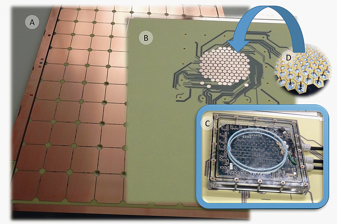
The measurement concept is based on the idea of being able to measure as directly as possible in the production process, to record the information of the local reaction rates as local flows and to be able to display them as live as possible in a spatially and temporally resolved manner. The basic idea of the development was that a sensor array is required to implement the idea, which must not differ in its external appearance (in contrast to available sensors [8] [9] [10]) from the actual processing object (panel, wafer), as any additional object in the electrolyte space in front of the panel or wafer will influence convection and field distribution and thus distort them. Therefore, the actual processing object must be replaced by a sensor array of the same format as far as possible for a measurement. The implementation of the concept is based on a cathodic current divider with integrated measuring resistors(Fig. 7). The copper outer layer of the measuring panel is divided into a series of individual segments. These are fed via vias to a rear-mounted measured value acquisition (resistance measurement), digitally processed and forwarded to a PC for visualization and storage.
, schematische Darstellung von Arrayanordnungen für Panel- und Waferformat (Mitte, rechts)") Fig. 7: Principle of single current measurement (left), schematic representation of array arrangements for panel and wafer format (center, right)
Fig. 7: Principle of single current measurement (left), schematic representation of array arrangements for panel and wafer format (center, right)
Various implementation variants were developed and tested; examples are shown in Figures 8, 9 and 10.
Figure 8 shows a test setup for optimizing the measurement process and determining parameters that influence convection. For the tests, the electronics were SMD-equipped on the back, and the sensor segments were electroplated with gold on an ENIG finish. A stabilized formate redox system was used as the measuring solution so that the properties of the sensor surface were not changed by the tests and various influencing variables could be investigated under comparable conditions. For example, the influence of cathodic aperture arrangements could be demonstrated in this system (as shown in Fig. 9 ).
By developing a spring contact adapter, suitably rewired 4-layer multilayers can be screwed directly to the 112-segment measurement electronics, which allows the measurement panels to be replaced at reduced cost and thus enables direct use in copper electroplating(Fig. 10).
 zur Erprobung des Sensorarrays mit Rückseiten-SMD-Bestückung (o.r.)")
 zur Erprobung des Sensorarrays mit Rückseiten-SMD-Bestückung (o.r.), Sensorarray mit Fertigungsrahmen/ Kurzschlussstruktur zur Vergoldung (u.l.), Fehlfarben-Stromverteilungsbild (u.r.)") Fig. 8: Swivelling 4″ test cell (top left) for testing the sensor array with backside SMD assembly (top right), sensor array with production frame/short-circuit structure for gold plating (bottom left), false color current distribution image (bottom right)
Fig. 8: Swivelling 4″ test cell (top left) for testing the sensor array with backside SMD assembly (top right), sensor array with production frame/short-circuit structure for gold plating (bottom left), false color current distribution image (bottom right)
") Fig. 9: Field diaphragm influence on the current distribution (ring diaphragms at 3mA/cm², diffuser flow rate 1.6 l/min)
Fig. 9: Field diaphragm influence on the current distribution (ring diaphragms at 3mA/cm², diffuser flow rate 1.6 l/min)
 Fig. 10: left: Adaptation of the 112-segment measuring electronics to full-format panel with exchange option center: Measuring insert copper electroplating in a vertical semi-automatic machine from Ramgraber right: False color distribution image, in the background measuring setup in use
4 Summary and outlook
The aim of this article was to illustrate correlations and prove them with suitable investigations that show the interaction between convection in the vicinity of the circuit substrate surface, the resulting diffusion layer thickness and the possible consequences for the heterogeneous interface reactions during etching and metal deposition as well as the superimposed influences of the electric field. Strong convection enables low diffusion layer thicknesses and high reaction rates, but quickly leads to non-uniformities across the panel surface due to the tendency to turbulence.
Using the examples of G-plating and direct flow with electrolyte recirculation, solutions for two different areas of application were presented.
More important, however, is the possibility for users to optimize existing systems themselves by determining the homogeneity of the process conditions across the panel surface under real conditions and optimizing them if necessary. The SILICET-UNIT is ideally suited for this purpose as a pivoting electroplating cell with adjustable process parameters, such as the flow direction, the distance from anode to cathode (adjustable in situ) and the position of anode to cathode within an adjustment range of 180° [11].
The newly developed system for local current detection and display was therefore presented and explained in this article. According to the authors, it offers the unique possibility of systematically optimizing galvanic and chemical process cells for various applications on planar surfaces.
In addition, the layout, measuring system and the materials to be used can be flexibly adapted to specific tasks.
Note
The project was funded by the Federal Ministry for Economic Affairs and Energy and the Central Innovation Program IZM
References
[1] N. Ibl: Oberfläche - Surface 14 (1973) 12, p. 367.
[2] P. Wingenfeld: Selektive Hochgeschwindigkeitsabscheidung von Edelmetallen in Bandanlagen, Teil 3; Galvanotechnik 1/ 2004.
[3] A. Spille-Kohoff: Simulation und Optimierung der Elektrolytströmung in der Galvanotechnik; ZVO Oberflächentage 2009 Bremen
[4] R. du Puits and C. Willert: The evolution of the boundary layer in turbulent Rayleigh-Bénard convection in air; Physics of Fluids 28, 044108 (2016); doi: 10.1063/1.4947261 (retrieved: 12.12.2023).
[5] R. Schmidt, M. Zwanzig, H. Moritz: Gravitationgestützte Galvanik zur Erzeugung 3-dimensional kristallin strukturierter Oberflächen; PLUS 6/2010.
[6] P.J. Köster et. Al.: Gold Shark Teeth Structures on MEAs - Electroplating of Nano-Structures on Metallic Micro- electrodes; Proceedings of the 7th International Meeting on Subs
rate-Integrated Micro Electrode Arrays, July 2008, Reutlingen, 289-290, ISBN-13 978-3-938345-08-5.
[7] US-Patent 2013/0186852 A1: Device and Method for Producing Targeted Flow and Current Density Patterns in a Chemical and/or Electrolytic Surface Treatment (retrieved: 12.12.2023).
[8] DE29817052U1 (retrieved: 12.12.2023).
[9] WO2006/093724A1 (retrieved: 12.12.2023).
[10] H. Mahdjour, P. Schwanzer, K. Schmid: Neues Verfahren: Real-time measurement of current density in the electroplating bath; Galvanotechnik 04/2013, pp. 712-725.
[11]https://www.silicet.de/ (Retrieved: 12.12.2023).
