Together with Chemnitz University of Technology and its Japanese partner Shinko Electric Industries Co., Ltd., Fhg ENAS has developed inductive bonding, a new joining technology for microsystems. It was presented at the MEMS Sensing & Network Systems 2022 in Tokyo at the end of January. The process is particularly revolutionary for the production of power electronics assemblies.
 Multichip assembly with all componentsTogetherwith the TU Chemnitz and the Japanese partner Shinko Electric Industries Co., Ltd. the Fhg ENAS has developed the new joining technology inductive bonding for microsystems. It was presented at the MEMS Sensing & Network System 2022 in Tokyo at the end of January. The process is revolutionary, especially for the production of power electronics units.
Inductive joining is a technology that has so far only been used for macroscopic components - examples include steel tubes or car doors. The joint development by the Fraunhofer Institute for Electronic Nano Systems ENAS in Chemnitz and its partners, Chemnitz University of Technology and the Japanese company Shinko, brings inductive joining to the micro level for the first time. For the mechanical surface contacting of chips on DBC (direct bonded copper) substrates, the bonding process was developed on the basis of sinter pastes with microsilver particles. Bonding processes of silicon chips on a DBC substrate were successfully carried out with such silver sinter pastes in the course of development.
With this process, various advantages can be utilized, especially in the heterointegration of chips and components:
- The inductive process enables very rapid heating of specific structures, for example bond pads, which are joined to the bond partner at a high local temperature.
- The temperature is mainly applied locally in the areas of the induction coils, so that the surrounding structures and components as well as the entire substrate are significantly less thermally affected by the very rapid heating and cooling of the local structures.
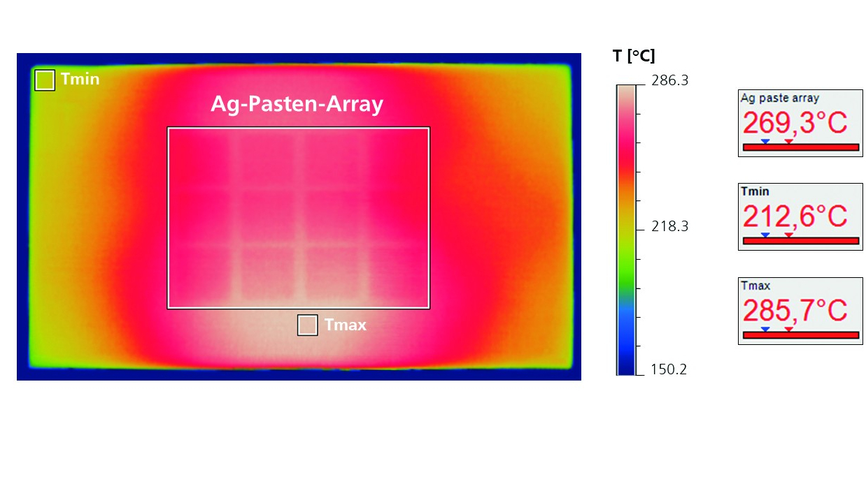
- With the help of induction coils, which are geometrically adapted to the bond structures, a high-frequency electromagnetic field induces eddy currents in the electrically conductive silver particle pad. Heating rates of more than 100 K/s were generated in this way.
- The overall process duration is significantly reduced with this method, as the target temperature of 300 °C is reached in just five seconds.
 Construction of the sintering module with the individual componentsAspart of the research work, a test setup was developed consisting of a process chamber with a sintering module, a pressure plate and an infrared camera for process monitoring. The sintering module contains a water-cooled induction coil in an electrically insulating surrounding material. The coil current and operating frequency were recorded in real time by means of process monitoring.
This process is revolutionary, especially for manufacturers of power electronics assemblies, as the duration of joining processes is significantly reduced and the thermal influence on all joining components is reduced. Mechanical contacting using silver sinter pastes allows the high waste heat from the components to be dissipated quickly and in a targeted manner via the sintered structures.
The Japanese development partner Shinko offers the process as an industrialized procedure and is continuously developing it further together with the project partners TU Chemnitz and ENAS.
The process was presented at the joint stand of Tohoku University and FhG ENAS at the MEMS Sensing & Network Systems 2022 trade fair, which took place from January 26 to 28 at the Tokyo Big Sight exhibition and event complex. A paper on inductive chip bonding can be requested via the following e-mail contact:
