In order to be able to use a plenoptic camera developed jointly with the South Korean KAIST and two specialized industrial partners in harsh industrial environments and to ensure a compact design, the electronics of the camera were miniaturized at Fraunhofer IZM using embedding technology.
Jointly with the south korean KAIST and two specialized industrial partners researchers at Fraunhofer Institute for Reliability and Microintegration (IZM) developed a special multi lens array camera. To use it in harsh industrial environments and to ensure a compact design, the camera's electronics were miniaturized at IZM using embedding technology.
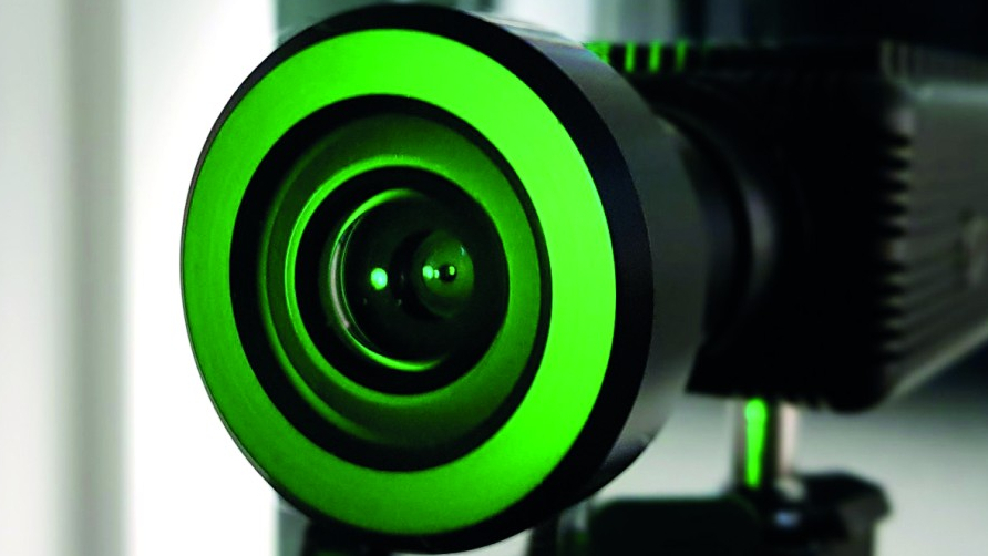
The high-speed camera, which is equipped with a multi-lens array and enables images with an extended depth of field, was developed by researchers at Fraunhofer IZM together with TecVenture, Optrontec Inc. and the renowned research institute KAIST. Thanks to miniaturized electronics, it is suitable for use in efficient damage analysis in industrial applications or for research purposes, for example.
With the acceleration of production processes in industry, the highest possible process control is desired at every step, which is why high-speed cameras are increasingly being used. However, when objects move in the image area, the focal plane cannot usually be readjusted so quickly. For this reason, cameras that have a greater depth of field with the same optics are advantageous. With such systems, the focal planes can be subsequently adjusted using the image data. Together with partners, researchers at Fraunhofer IZM have set themselves the goal of developing and constructing miniaturized camera systems of this kind as high-speed cameras.
Depending on the application, the camera is fitted with an appropriate lens and the image is focused on a full-format sensor. A multi-lens or polarization filter array developed by KAIST and Optrontec in Korea is placed in the beam path between the image sensor and the lens. This enables a greater depth of field or higher contrast for structural details of the observed object. The recording speed of 2000 images per second is up to 10 times faster than with conventional cameras. This makes very fast and critical processes in industrial production or research accessible for detailed visual analysis.
The microlens array (MLA) consists of an array of densely arranged lenses that are 150 micrometers apart. The components required to power the image sensor are highly integrated below the sensor in an embedded module.
In addition to the considerable miniaturization of the electronics through the embedding of electronic components in the PCB and 3D stacking, the electrical connections can also be shortened. This increases the quality of the transmitted signal, particularly in high-speed systems. The electronics are very robust, not least because they are now largely encapsulated. This highly integrated electronic module was built in the Fraunhofer IZM's PCB production department.
The optimized performance of the camera has already been demonstrated in the first functional tests. In further work over the next few months, the manufacturing processes will be refined and transferred to an industrial process. The plenoptic high-speed camera can not only be used for industrial process analysis, the combination of speed and depth of field is also extremely interesting for scientific investigations of biological, chemical or physical processes. The project is funded by the German Federal Ministry for Economic Affairs and Energy as part of the German-Korean research cooperation through the ZIM funding program.
The German partner TecVenture is a development company in the field of embedded systems based in Leipzig. It consists of an engineering office and a manufacturing company and has been responsible for numerous electronic assemblies and devices as well as the necessary firmware and software since 1993. Customers can be found in a wide variety of technology sectors; well over a hundred projects have been realized. A particular focus is the development of safety-critical applications.
The South Korean partner Optrontec was founded in 1998 and is now one of the most important specialists for optical-electronic systems. The company has now focused on three fields of application: Cameras and optical systems for mobile applications, for automotive and for security technology. The company is headquartered in Pangyo (Seoul region); production sites are located in South Korea (2), China (2) and Vietnam (1).
http://en.optrontec.net,http://tec-venture.de www.kaist.ac.kr, www.izm.fraunhofer.de
