
In aviation technology, components and even entire systems are traditionally designed hierarchically according to the principle 'one function = one part'. However, in order to increase passenger comfort in the cabin in particular, a constantly increasing range of functions must be realized today without simultaneously increasing the volume and, above all, the mass of the components disproportionately. This calls for new concepts. As part of the 'Component 4.0' research project, a design concept was developed for a highly integrated and functionalized lightweight component for the aircraft cabin. A test vehicle for such a lightweight component was designed for this concept, whereby a simple energy and data supply was initially considered. The assembly and connection technology for the electronics was developed close to industrial standards - taking into account that this electronics module must be integrated into the lightweight component. A test principle was developed and implemented to evaluate the reliability and safety of the lightweight component as a whole, as well as the electronics. These tests were modeled and simulated using the finite element method (FEM), so that virtual simulation tests can also be used to estimate the reliability or component failure of modeled lightweight assemblies with integrated electronic modules.
In aerospace engineering, components and even entire systems are traditionally designed hierarchically according to the principle 'one function = one component'. However, in order to increase passenger comfort in the cabin in particular, a steadily increasing range of functions must be realized today without at the same time disproportionately increasing the volume and, above all, the mass of the components. This calls for new concepts. As part of the 'Bauteil 4.0' research project, a design concept was developed for a highly integrated and functionalized lightweight component for the aircraft cabin. For this concept, a test vehicle of such a lightweight component was designed, initially considering a simple energy and data supply. The assembly and connection technology for the electronics was developed close to industrial standards - taking into account that this electronics module has to be integrated into the lightweight component. A test principle was developed and implemented to evaluate the reliability and safety of the lightweight component as a whole, as well as the electronics. These tests were modeled and simulated using the finite element method (FEM), so that virtual simulation tests can also be used to estimate the reliability or component failure of modeled lightweight assemblies with integrated electronics modules.
Project history and motivation
![Abb. 2: Darstellung aus dem Video „Imagine Innovations Flying Tomorrow“ von Airbus und dem Cabin & Cargo Netzwerk des Bundesverbandes der deutschen Luft- und Raumfahrtindustrie zu aktiven Oberflächen [2]](/images/stories/Abo-2022-04/plus-2022-04-0038.jpg "Abb. 2: Darstellung aus dem Video „Imagine Innovations Flying Tomorrow“ von Airbus und dem Cabin & Cargo Netzwerk des Bundesverbandes der deutschen Luft- und Raumfahrtindustrie zu aktiven Oberflächen [2]") Fig. 2: Illustration from the video "Imagine Innovations Flying Tomorrow" by Airbus and the Cabin & Cargo Network of the German Aerospace Industries Association on active surfaces [2]In the past decade, the Federal Ministry of Education and Research (BMBF) has supported supra-regional cooperation and networking between competence centers in Germany with the funding program 'Zwanzig20 - Partnership for Innovation', among other things. In particular, expertise from aerospace development was also pooled with a focus on electronics and semiconductor technology. The 'Energy Efficient Aviation Solutions (EEAS)' project was not primarily concerned with technical project work, but with networking the relevant companies in the regions and the research institutions from the previously separate networks 'Berlin-Brandenburg Aerospace Allianz (BBAA e. V.)', 'Hamburg Aviation e. V.' and 'Luft- und Raumfahrttechnik Sachsen/Thüringen e. V. (LRT)' on the subject of aviation research and technology on the one hand and the 'Silicon Saxony' network on the subject of 'electronics and electronics integration' on the other. The Center for Microtechnical Production at TU Dresden, which had already carried out initial feasibility studies on the integration of electronics, was also involved. Building on this, the idea for the project 'Functionally integrated sandwich components for the aircraft cabin as a prerequisite for Industry 4.0 and innovative operating and MRO processes' (acronym 'Bauteil 4.0') was born and finally approved as a cooperation project between the three institutions IMA Materialforschung und Anwendungstechnik GmbH Dresden, Hamburg University of Technology, Institute of Aircraft Cabin Systems, and Dresden University of Technology, Center for Microtechnical Production, in the 3rd call of the Aviation Research Program V (LuFo V-3) of the Federal Ministry for Economic Affairs and Energy (BMWi).
Fig. 2: Illustration from the video "Imagine Innovations Flying Tomorrow" by Airbus and the Cabin & Cargo Network of the German Aerospace Industries Association on active surfaces [2]In the past decade, the Federal Ministry of Education and Research (BMBF) has supported supra-regional cooperation and networking between competence centers in Germany with the funding program 'Zwanzig20 - Partnership for Innovation', among other things. In particular, expertise from aerospace development was also pooled with a focus on electronics and semiconductor technology. The 'Energy Efficient Aviation Solutions (EEAS)' project was not primarily concerned with technical project work, but with networking the relevant companies in the regions and the research institutions from the previously separate networks 'Berlin-Brandenburg Aerospace Allianz (BBAA e. V.)', 'Hamburg Aviation e. V.' and 'Luft- und Raumfahrttechnik Sachsen/Thüringen e. V. (LRT)' on the subject of aviation research and technology on the one hand and the 'Silicon Saxony' network on the subject of 'electronics and electronics integration' on the other. The Center for Microtechnical Production at TU Dresden, which had already carried out initial feasibility studies on the integration of electronics, was also involved. Building on this, the idea for the project 'Functionally integrated sandwich components for the aircraft cabin as a prerequisite for Industry 4.0 and innovative operating and MRO processes' (acronym 'Bauteil 4.0') was born and finally approved as a cooperation project between the three institutions IMA Materialforschung und Anwendungstechnik GmbH Dresden, Hamburg University of Technology, Institute of Aircraft Cabin Systems, and Dresden University of Technology, Center for Microtechnical Production, in the 3rd call of the Aviation Research Program V (LuFo V-3) of the Federal Ministry for Economic Affairs and Energy (BMWi).
Inspired by highly functionalized construction components in the automotive industry (see e.g. Fig. 1), the development of multifunctional lightweight components for aviation technology is an obvious consequence. Highly functional and thus highly integrated lightweight components have great potential for optimizing weight and increasing passenger comfort. The reliability and safety requirements from the automotive industry are generally even higher in aviation technology. These high demands on functional safety ultimately result in a strict separation of functions for individual components in an aircraft according to the principle 'one function = one component'.
In contrast to the components and systems in the cockpit of an aircraft, the requirements for reliability and safety in the aircraft cabin are slightly reduced and therefore more comparable with the requirements from the automotive industry. In the automotive industry, it has already been sufficiently proven that integrating functions into structural components, e.g. for data and energy transmission, can meet the strict requirements in terms of resilience and also offers the potential to make production, assembly and maintenance processes more intelligent and simpler (keyword "Industry 4.0").
![Abb. 3: MAVERIC CABIN, Studie von Airbus zur künftigen Gestaltung der Kabine [3]](/images/stories/Abo-2022-04/plus-2022-04-0039.jpg "Abb. 3: MAVERIC CABIN, Studie von Airbus zur künftigen Gestaltung der Kabine [3]") Fig. 3: MAVERIC CABIN, study by Airbus on the future design of the cabin [3]
Fig. 3: MAVERIC CABIN, study by Airbus on the future design of the cabin [3]
Aircraft manufacturers and their suppliers have been developing visionary concepts on this topic for a long time. Particularly in the cabin area, the focus is on increasing the range of functions and comfort for passengers(Fig. 2 and Fig. 3). In view of the special requirements for electronic assemblies in aviation, fundamental questions must first be clarified. The very strict approval requirements and extensive approval processes often only allow small development steps and are usually the reason for a comparatively conservative attitude on the part of manufacturers when it comes to actual implementation.
From the perspective of the project consortium, the following fundamental questions therefore had to be answered:
- How can electronic modules of varying complexity be integrated into the manufacturing process of typical cabin components?
- What loads are these embedded electronic modules exposed to during operation?
- To what extent do the embedded electronic modules influence the stability of the cabin components?
- What concepts are conceivable for designing functionally integrated cabin components that are suitable for assembly and maintenance with regard to the embedded electronics?
Production of typical cabin components
For climate-friendly and efficient flying, lightweight construction to reduce weight has always been the decisive factor in the design of aircraft and cabin components. Even in today's modern and economical long-haul aircraft, saving one ton of empty weight results in fuel savings of around 0.45%. Depending on the range of use of the aircraft, this would be 0.1 to 0.3 tons/flight. In an aircraft's lifetime, this is around 2000 tons less kerosene consumption, which is equivalent to saving 6300 tons ofCO2.
![Abb. 4: Sandwichbauteil in Wabenbauweise [4]](/images/stories/Abo-2022-04/plus-2022-04-0040.jpg "Abb. 4: Sandwichbauteil in Wabenbauweise [4]") Fig. 4: Sandwich component in honeycomb construction [4]
Fig. 4: Sandwich component in honeycomb construction [4]
The lightweight components in the cabin are almost exclusively sandwich components (referred to as 'sandwich components' in the rest of the document). Such components(Fig. 4, A) are usually manufactured in the cabin as a laminate of CFRP (carbon fiber composite) or GFRP (glass fiber composite) cover layers(Fig. 4, B) and a so-called Nomex honeycomb as the core(Fig. 4, C). Nomex honeycombs consist of aramid paper impregnated with phenolic resin. These layers(Fig. 4, B-C-B) are bonded together under pressure and temperature to form the sandwich component(Fig. 4, A). The temperature is applied in the form of a ramp in a heating and cooling phase. A distinction must be made between the production of molded sandwich components in an autoclave with the support of negative pressure and heat and the production of flat sandwich panels in a heated press. Typical molded components are, for example, side wall panels and canopy panels. Flat panels are used as floor panels or in the production of galleys or lavatories and their doors.
In the course of the project, samples of such panel-shaped components were manufactured using the equipment available in the production process of a manufacturer of cabin components (3D ICOM GmbH & Co. KG, Hamburg) and thus under product-identical conditions. The following process parameters were used and provide an impression of the load conditions that act on these modules during the production process due to the embedding of electronic modules in sandwich components:
- Pressure in the press up to 1.9 MPa, whereby an aluminum forming tool manufactured to undersize limits the final height (thickness) of the sandwich component,
- Heating gradient [3-5] K/min
- Peak temperature [120-135] °C with a holding time of 1 h-2 h
- Cooling gradient: [-3-5] K/min.
It is clear from the parameters that an additional electronic module to be embedded is already subjected to a not inconsiderable mechanical-thermal load during the manufacturing process.
Concept of a test vehicle
In view of the manufacturability of the sandwich components with integrated electronics and the validation of the numerical models, which was carried out using FEM, it was necessary to start with a geometrically simple design of the test specimens. The original project concept of integrating highly functional input and output devices into a lightweight component was abandoned in favor of integrating a simple RFID component into a sandwich construction part after a corresponding analysis of the problem. The background to this was the approach that a scaling of easily comprehensible and conclusive results from simple structures to complex structures is easier to realize than an extensive simulation of a highly integrated lightweight component.
Important boundary conditions must be considered from two sides in particular. On the one hand, the view of the lightweight component and its design requirements for mechanical stability must be considered. This must be guaranteed as a prioritized and original function without restriction. This means that the introduction of an additional component, i.e. the electronics, must initially be regarded as a point of failure, which must not affect the reliability and safety of the lightweight component to such an extent that it falls into a critical area. Secondly, the function of the electronic component itself must be safeguarded over the entire service life of the sandwich component. The insertion of the electronics into the lightweight component also results in a change to the previously known load scenarios on electronic components. In particular, mechanical stresses and vibrations act to a greater extent and in a different distribution than is the case under traditional load scenarios for electronic assemblies.
 versus eingebettet (EC)") Fig. 5: FEM simulation of the load on a ceramic two-pole in surface mounting (SMT) versus embedded (EC)
Fig. 5: FEM simulation of the load on a ceramic two-pole in surface mounting (SMT) versus embedded (EC)
This behavior is already known from earlier studies on the embedding of electronic components, e.g. in printed circuit boards. Figure 5 shows on the left the FE models of a two-terminal component in surface mounting and embedded in the inner layer of a printed circuit board. Both were subjected to a simulation in which they underwent thermal cycling from -40°C to 125°C. The diagrams on the right show that the two-pole solder meniscus (yellow-colored volume discretized with 3D elements in the middle illustration) is subjected to tensile stress at low temperatures and slight compressive stress at high temperatures both in surface mounting (SMT) and in embedded mounting (EC). In the stand-off of the solder joint (grey-coloured volume discretized with 3D elements in the middle illustration), both assembly variants behave completely differently. In the surface-mounted two-pole solder joint, the stresses are built up in the opposite direction to the temperature level in the tensile direction, as in the meniscus, whereas in the embedded component they are built up in the same direction as the temperature, but only in compression.
Assembly and connection technology of the electronic components
") Fig. 6: Layout of the RFID tag, assembled daisy chain and assembled RFID chip (from left to right)In a first iteration, a test coupon, designated V0 in the project, was to be constructed. This was to offer the possibility of being able to prove its functionality 'live' inside the sandwich component later during load tests. A solution in the form of an RFID tag that can be queried at any time with the help of an appropriate reader was therefore the obvious choice. In addition, it should also be possible to measure a continuous electrical parameter in situ if required.
Fig. 6: Layout of the RFID tag, assembled daisy chain and assembled RFID chip (from left to right)In a first iteration, a test coupon, designated V0 in the project, was to be constructed. This was to offer the possibility of being able to prove its functionality 'live' inside the sandwich component later during load tests. A solution in the form of an RFID tag that can be queried at any time with the help of an appropriate reader was therefore the obvious choice. In addition, it should also be possible to measure a continuous electrical parameter in situ if required.
Thin substrate materials were used for the RFID tag in order to keep the 'interference point electronic module' in the overall structure of the sandwich component as small as possible during this phase. The thickness varied from 0.1 mm to 0.4 mm in order to characterize the possible influence of a change in stiffness. For the functionality of the RFID chip, different antenna designs were examined with regard to their size. The writable RFID chip SL3S1003 from NXP was selected. NXP also provides three antenna designs with different sizes and therefore different qualities and ranges. The range is important for two reasons. Firstly, the influence of the location of the electronics embedding should be investigated. For this purpose, it may be necessary to be able to measure the RFID chip through a lightweight assembly if the chip is on the back of the sample. On the other hand, it may also be possible to measure in limited installation spaces. Based on these considerations, the largest of the proposed antennas for the target design was already defined after the first tests. The assembly and connection technology was carried out using a standardized SMD process. An eight-fold panel was used to increase productivity. A type 3 SnAg3Cu0.5 solder paste was used for the contacting. This was printed automatically using a stainless steel stencil (thickness 100 µm). Placement was also automated. The subsequent soldering process was carried out in a five-zone convection oven in a normal atmosphere. For reliability tests, a daisy-chain resistor chain with 0 ohm resistors of type 0201 was integrated for the electrical measurement, with one measurement contact per measurement series being routed to the outside. Figure 6 shows the layout and the two installation situations.
 Fig. 7: PCB panel with tear-off fabric applied on one sideTheelectronic modules must be constructed in a suitable manner for integration. Compatibility of the components must be ensured, especially with regard to the materials. As described above, integration takes place in a press, whereby the Nomex honeycomb core is pressed on both sides with a top layer of phenolic resin and cured. To integrate the electronic modules, an additional prepreg layer of phenolic resin is applied in the area of the modules so that they are surrounded by phenolic resin on both sides. Experience has shown that a phenolic resin prepreg and fully cross-linked epoxy resin form a very secure bond when curing. With regard to the electronic module, this means that the use of typical flex PCB materials was deliberately avoided and instead standardized and very thin (see above) FR4 material was used, which bonds ideally with phenolic resin. Additional materials such as solder resist were also dispensed with. For better bonding, it is also necessary to laminate a so-called peel ply onto the electronic module, which is only torn off directly before embedding and gives the surface a certain roughness and structure on the one hand and activates the surface on the other. This additionally improves the bonding of the phenolic resin system to the FR4 material. The tear-off fabric was laminated in a PCB press with a standardized FR4 prepreg, but with adapted process parameters, in particular with a significantly reduced pressing force of approx. 0.1 MPa.
The positive effect of the peel ply was verified by measurement on a more complex electronic module used later (which will be discussed below) Figure 8 on the left shows a section of the topography measurement on the back of an electronic module in its original state. The roughness is in the single-digit micrometer range (Ra = 0.12 µm; Rz = 1.7 µm). After tearing off the fabric (Fig. 8 right), a clear surface structure can be seen, which is only comparable to a natural roughness to a limited extent. Height differences of up to approx. 50 µm occur here.
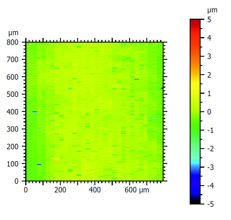
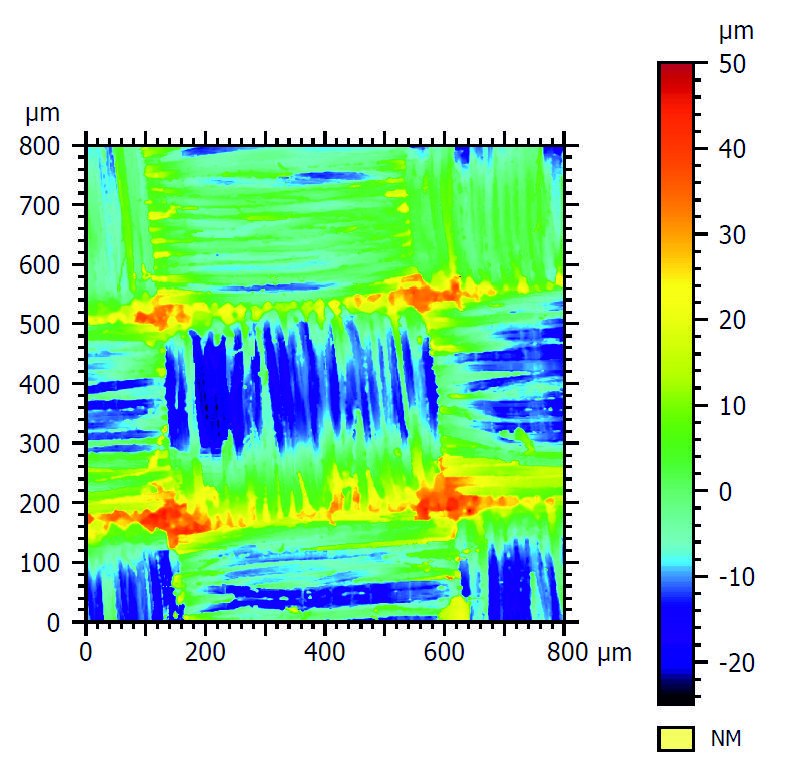
Fig. 8: Topography on the back of an electronic module in its original state (left) and after tearing off the previously applied peel ply (right), note the different scaling of the color scales!
Development of a test stand
In the project, mechanical loads on sandwich components with integrated electronic modules were initially to be considered. Load scenarios were analyzed for the development of a suitable test stand. Generally applicable standards for carrying out such tests are only used in isolated cases, e.g. for bending tests [5]. Instead, each aircraft manufacturer specifies which component should withstand which loads without damage. For example, a manufacturer of side wall panels and partition walls (these are the partitions between the seating areas in the cabin) states that for a panel measuring approximately 180 cm x 180 cm, a force of 680 N (approx.70 kg) at the load-critical point, the deflection must not exceed 25 mm. For partition walls, the maximum deflection is 25 mm at a force of 900 N (approx. 92 kg). With the geometric parameters mentioned, the maximum permissible deflection of 25 mm results in a bending radius of approx. 16.2 m. These values had to be compared with our own later measurements. The regulations for floor slabs are less precise. Here, for example, the following criterion is stated: "No perceptible deflection with a load of approx. 900 N over a span of 470 mm".
The following load cases were derived from these and other specifications in company standards:
- flat application of force on the sandwich component to deflect it (4-point bending test)
- point load application by means of a pressure spherical cap with a radius of 5 mm (e.g. shoe heel on floor slabs)
- point load application by means of a compression spherical cap with a radius of 37.5 mm (e.g. ball of the hand resting on a tray table).
The test stand therefore had to be able to be operated in two modes (see Fig. 9).
 Fig. 9: Principle sketch of the two test stand modes, top: Four-point bending, bottom: Point loading
 Fig. 10: Test stand, here set up for the 'four-point bending' modeFor both load cases or modes, the forces applied are checked using a load cell. In the case of four-point bending, the deformation achieved is also recorded by a displacement transducer. Figure 10 shows the realized setup of the test stand. The displacement transducer is located centrally below the test specimen. With a point load, the condition of the specimen is characterized after loading.
For initial verification of the test stand and to determine initial values for later measurements, point loads were applied to dummy samples. These were unused edge areas or sections of real panels, so that these samples have comparable mechanical properties to the lightweight panels actually used. Figure 11 on the left shows the dummy specimen. Three different forces were applied to the sample with each of the two pressure pads (radii 5 mm and 37.5 mm and diameters 10 mm and 75 mm).
The qualitative results of these tests are listed in Table 1. With the larger compression dome, a visible impression in the surface layer was only visible at a force of 500 N. With the smaller pressure pad, the visible impression was already made at the lowest applied force of 100 N. The impressions can be seen on the right-hand side of Table 1 in the backlight images. This result confirmed the assumptions made in advance and provided reference points for subsequent tests as part of the project.
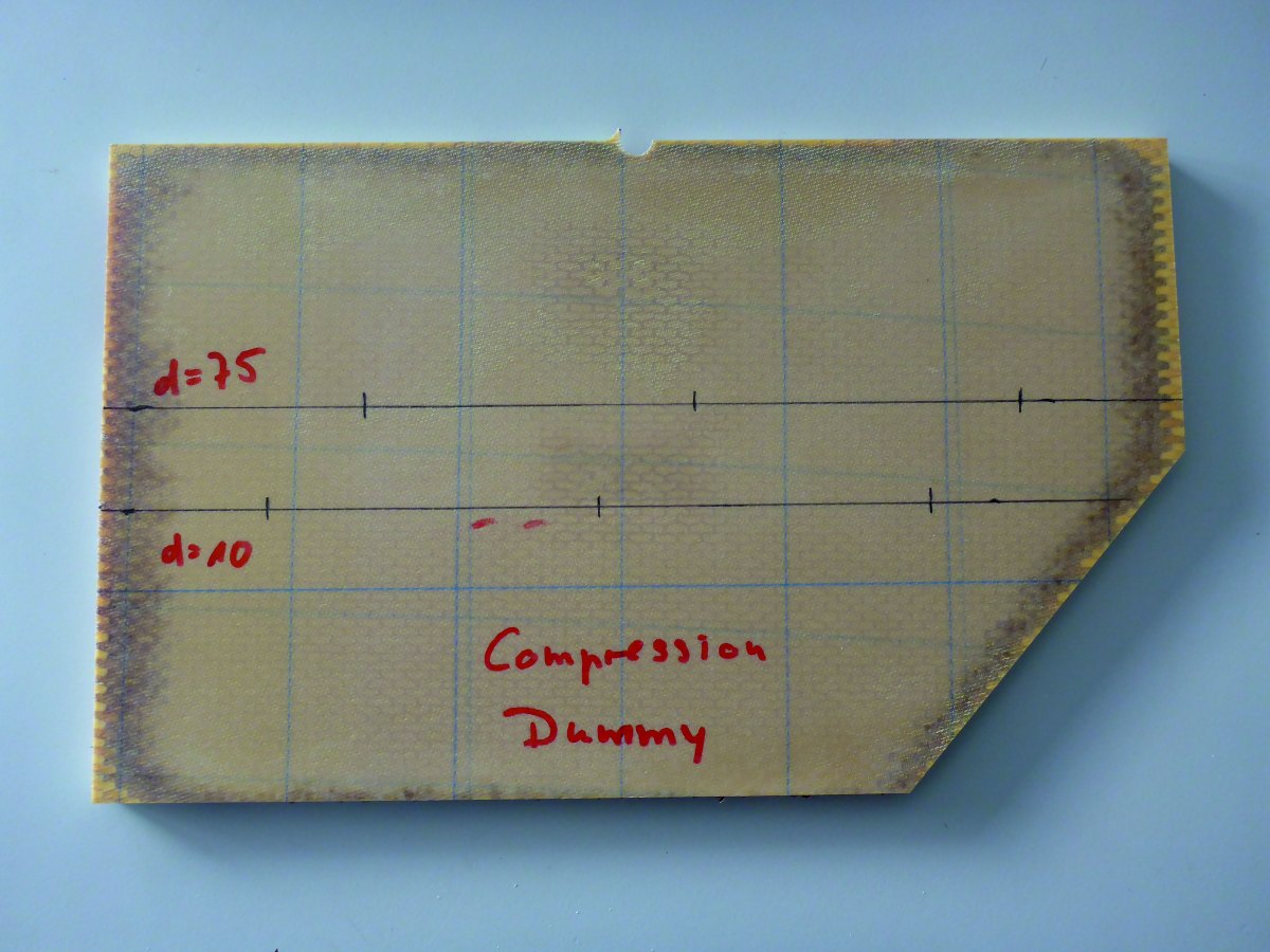
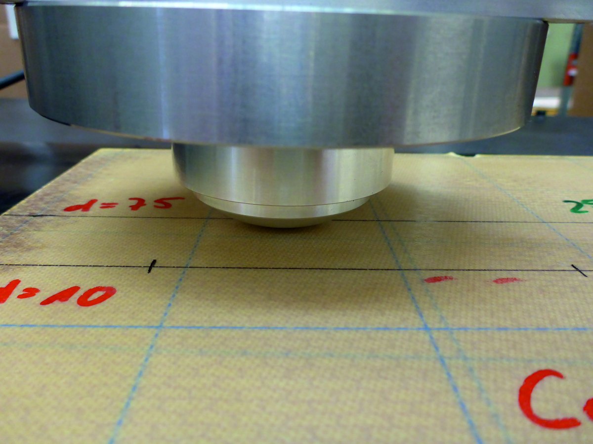
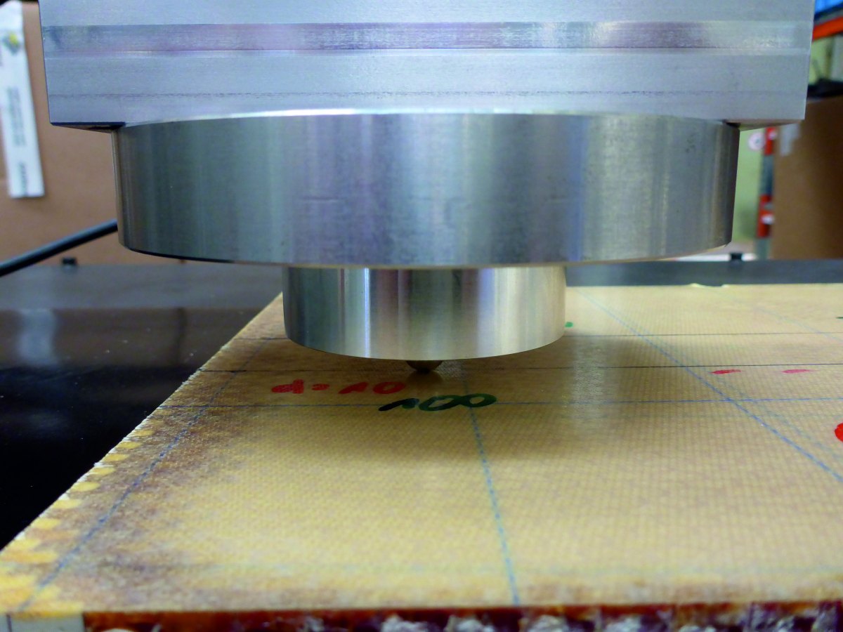
Fig. 11: Left: Dummy for point loading with marked load points Center: large pressure dome on top Right: small pressure dome on top
| Diameter of pressure dome d = 75 mm F = 100 N => no visible impression F = 250 N => no visible impression F = 500 N => visible impression |
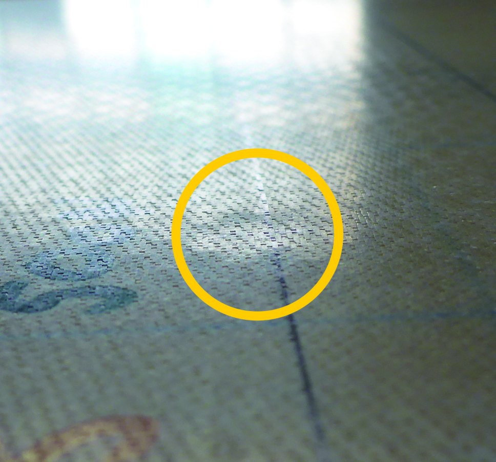 |
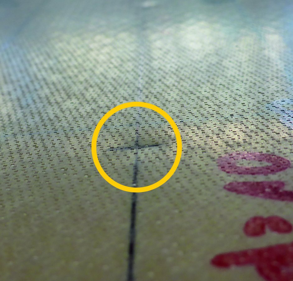
| Diameter of pressure dome d = 10 mm F = 100 N => visible impression F = 200 N => visible impression F = 400 N => visible impression |
 |
Sample production
Adapted to the possibilities of the designed test stand, the first samples were manufactured on production systems from the lightweight component manufacturer 3D ICOM. As explained above, the honeycomb and cover layers are stacked accordingly and laminated in a press in a heating and cooling process under pressure.
The test vehicles were manufactured using an aluminum frame mold to limit the outer dimensions in order to prevent the fabric from slipping and the Nomex honeycomb core from being pressed in. In a first iteration, 25 mm high test vehicles were produced, consisting of two cover layers, the Nomex paper honeycomb and the embedded electronic component. The test vehicles each had a width of 100 mm and a length of 350 mm.

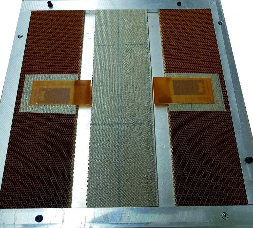
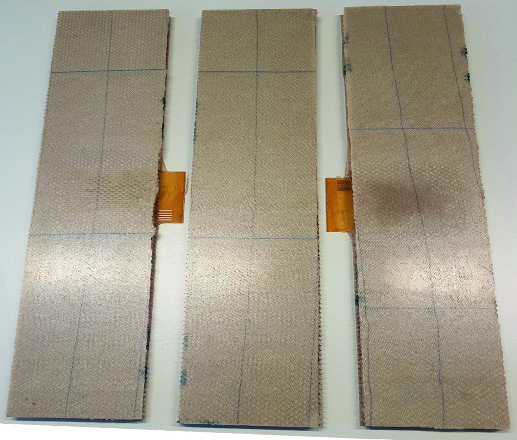
Fig. 12: CAD model of the press device, laid layer structure, pressed samples (from left to right)
Figure 12 on the left shows the CAD model of the aluminum frame mold with inserted samples. The test vehicles were each produced in sets of three, two test vehicles on the left and right with integrated electronics and one test vehicle in the middle without a disturbance as a reference for the component behavior. This meant that test vehicles with and without embedded electronics were available for all subsequent tests, each of which underwent the identical production process with the same process variables. Figure 12 shows the unpressed layers in the middle and the finished samples on the right after pressing. The RFID tags embedded in the left and right samples are clearly visible, the middle sample without embedded electronics. Typical materials and material thicknesses from the aircraft cabin were used for the manufactured lightweight component in order to ensure the greatest possible comparability. The specific layer structure and the materials used are shown in the following list:
- Top cover layer: two layers of Gurit PHG600-68-50 [6]
- Honeycomb layer: Schütz Coremaster C1 - 4.8 honeycomb hexagonal 24.5 mm high in the W direction [7]
- Additional layer as base for test vehicle: Gurit PHG-600-68-50 [6]
- Test vehicle: Electronic module
- Top layer at the bottom: 2 layers of Gurit PHG600-68-50 [6]
The design of the lightweight component was deliberately kept simple, as was the design of the integrated electronic components to reduce interference factors in testing and simulation.
 Fig. 13: W and L direction for the honeycomb layer
With regard to the honeycomb position, it should be noted that it has two orientations, the W direction and the L direction (Fig. 13). The W direction is the mechanically weaker direction due to the bonding of the cells to the nodes. It was therefore mainly placed in the longitudinal direction to the samples in order to enable appropriate deformation during the bending tests.
The samples were analyzed and evaluated after assembly. The electrical functionality was used as the first basis for evaluation. For this purpose, the RFID chips were read and in some cases also described. The daisy chains were measured electrically for resistance. Resistances in the range of up to 10 ohms were measured for a resistance chain.
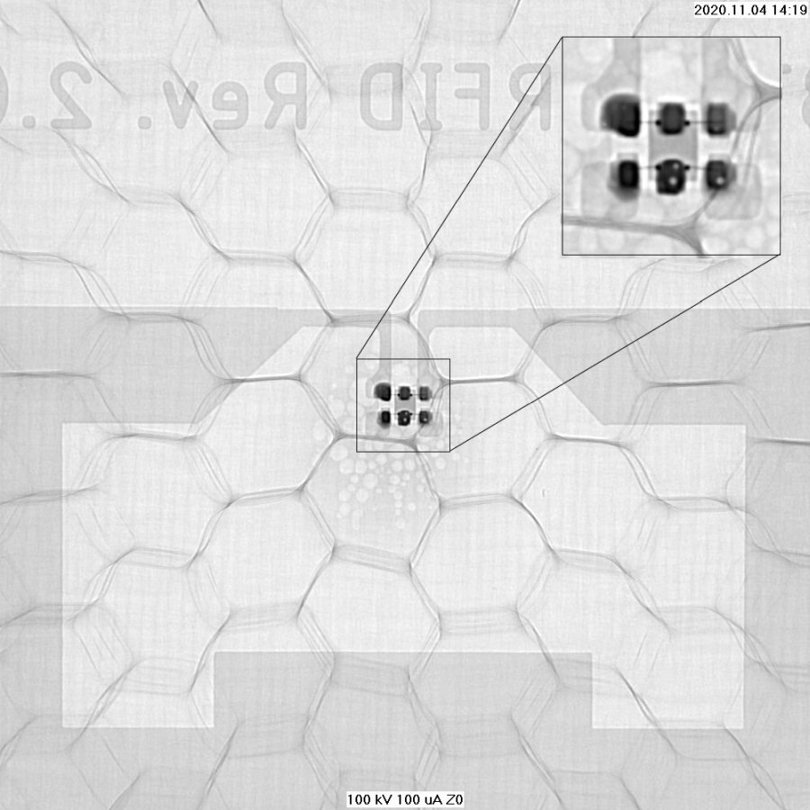
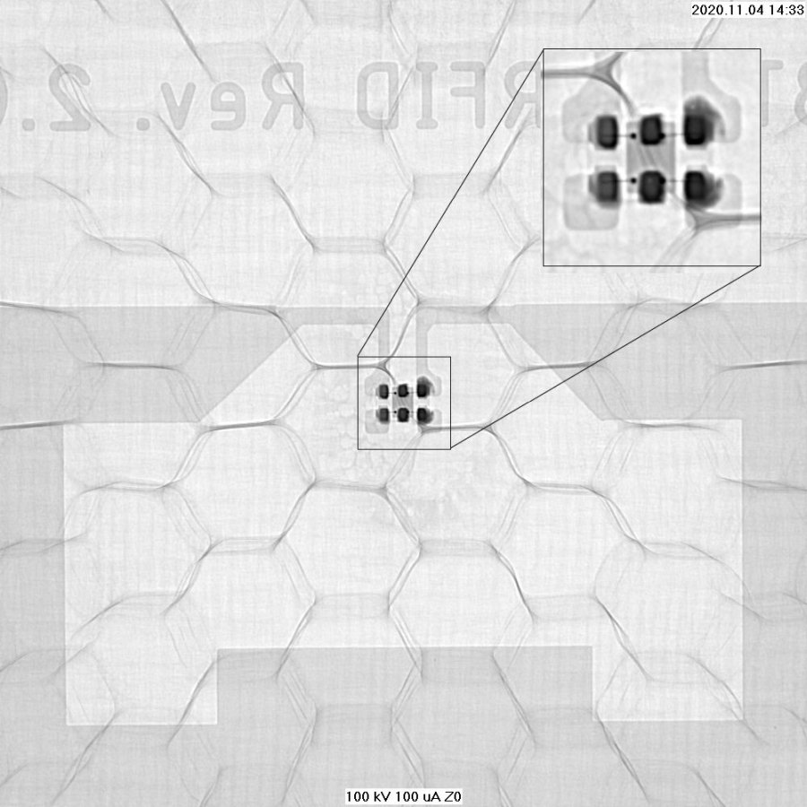
Fig. 14: X-ray analysis of RFID components; left: Honeycomb edge on the edge of the RFID component, right: honeycomb edge hitting the RFID component directly
The structure was also examined non-destructively. X-ray microscopy was used for this purpose. Due to the high proportion of design-related air inclusions and the material combination itself, ultrasound microscopy is not sufficiently suitable for analyzing defects or even the properties of the structure. X-ray microscopy, on the other hand, is very suitable. With adjusted parameters, it is possible to analyze both the electronics and the honeycomb structure. It was shown that no significant structural changes were caused by the manufacturing process. However, it was observed that some RFID components came to rest directly on a honeycomb edge. They were still functional after production. However, this circumstance can lead to a reduction in reliability, especially with regard to the electronics, as higher and undefined voltages may occur here. A slight displacement of the honeycomb edges in the area of the embedded electronics was also observed. A significant influence of these irregularities on the reliability could not be proven in the following load tests.
Bending and compression tests
The manufactured test specimens (thickness approx. 25 mm) were subjected to the four-point bending test on the designed test stand. In a first test, a specimen without embedded electronics was subjected to an increasing load up to 500 N. Figure 15 shows a close-up of the specimen in the test stand. Figure 16 shows the progression of force and deformation.
 Fig. 15: Close-up of the first specimen in the test stand
 Fig. 16: Force and displacement curve for test 1Thefigures show that a maximum deflection of 0.84 mm was achieved at a load of 500 N. Converted, this means an (average) bending radius of approx. 15.3 m. This test is therefore within the range of the specifications quoted above in the text. It can be concluded from this that even a sandwich panel of this thickness (25 mm) with the relatively simple layer structure is sufficiently resistant to the standard loads so that the resulting deformation will not have any critical effects on the embedded RFID tags. This sample was then used for preliminary tests of dynamic loading, i.e. cyclic load application. The aim was to define suitable cycle times for subsequent tests.
The subsequent test was the dynamic load on a panel with an embedded RFID tag. The functionality of the RFID component was checked periodically using a corresponding RFID reader.
The test was carried out in several sub-steps. First, 500 cycles were run in which the sample was placed in the test stand so that the RFID tag was aligned downwards and thus subjected to tensile stress during deflection, see example with other sample in Figure 18. The sample was then rotated 180° along the horizontal axis so that the RFID tag was aligned upwards and thus subjected to compressive stress, see example with other sample in Figure 19. A total of 2000 cycles were carried out in this alignment. The sample was then rotated 180° again and subjected to another 1500 cycles. In total, this specimen was subjected to 3500 cycles. No damage or functional impairment of the RFID tag was observed.
 Fig. 17: Side view of the sample, RFID tag on top
Compression tests were also carried out on the test specimens with a thickness of 25 mm. Figure 17 shows red markings in the area of the RFID tag. During the characterization of the samples after their production, the position of the RFID chip was also determined and marked by means of X-ray examination in order to apply the load in this critical area during compression tests. Loads of 200 N to 1000 N were applied using the 75 mm diameter pressure calotte. Even after applying a force of 1000 N, the RFID tag was still functional. With the 10 mm diameter spherical cap, visible marks were made on the surface of the test specimen from 700 N at the latest.
 Fig. 18 left: Damage case with RFID tag at the bottom, crack in the top cover layer
 Fig. 18 right: Damage case with RFID tag on top, crack in bottom top layer
The difference to the previous test with the small spherical cap, in which visible impressions already occurred from 100 N, can be explained by the double top layer in the current 25 mm thick test specimens.
As a consequence of the bending tests described above, which were without any damage, the layer structure of the test specimens was changed in the next step to allow for larger deformations. The test rig was also modified accordingly for higher loads. By reducing the number of outer layers (which reduces the stiffness of the component) and using a thinner honeycomb layer, the new specimen structure only had a thickness of approx. 10 mm. The honeycomb layer was used in both the W and L directions.
- Top cover layer: one layer of Gurit PHG600-68-50 [6]
- Honeycomblayer: Schütz Coremaster C1 - 3.2 honeycomb hexagonal 9.5 mm high in the W and L direction [7]
- Additional layer as base for test vehicle: Gurit PHG-600-68-50 [6]
- Test vehicle: Electronic module
- Top layer at the bottom: one layer of Gurit PHG600-68-50 [6]
The subsequent test was intended to investigate the load-bearing capacity of the modified thinner specimens. It was found that the maximum possible deformation of approx. 15 mm was reached in the existing test setup at a load of 870 N due to the design. The test stand first had to be adapted accordingly. This meant that significantly more suitable deformation data was already available as input information for simulating the component in the fixture.
In the test session with the modified setup, a sample without an embedded electronic module was examined first. The qualitative course of the deformation from the preliminary test up to 870 N load could be reproduced. These results were therefore confirmed once again. The load was then increased further until the specimen failed, which occurred at a load of approx. 1150 N and a deflection of 20.6 mm. When the component failed, the top cover layer had detached. The next test involved a sample with an embedded RFID tag, in this case aligned downwards, i.e. subjected to tensile stress. The failure occurred at approx. 875 N and a deflection of 14.5 mm. The upper cover layer was torn(Fig. 18). Nevertheless, the RFID tag was still functional after the damage.
A further test with the RFID tag in the direction of pressure was carried out without any abnormalities up to a load of approx. 1100 N and a deflection of 21 mm. After this, damage occurred to the lower cover layer(Fig. 18 right).
In summary, it can be stated that the load applied to embedded RFID tags was apparently relatively low, even at unusually high loads for a selected construction (the deflections achieved are far above what would be acceptable for a selected sandwich structure), as all RFID tags were still readable after the tests. The test part therefore fails structurally before any damage to the RFID tag would occur. The electronics only fail during breakage if an additional point load acts directly on the electronics during failure. Deflections of 15.8 mm were achieved with the 10 mm high samples in the four-point bending test at a load of 872 N. This corresponds to an extreme bending radius of approx. 82 cm and a bending moment of approx. 70 Nm.
FE analyses
Based on the findings of the first bending tests, a concept of complex modeling of an embedded electronic module in interaction with the surrounding sandwich structure, which had been pursued in the meantime, was initially postponed. Such detailed and thus complex modeling of both the electronics and the sandwich component would have exceeded the available project resources and should therefore be reserved for a possible follow-up project.
The simulation approach was therefore simplified in terms of its complexity by considering the embedded electronics as a 'black box' and only modeling it as a corresponding fault location with homogeneous properties in the sandwich structure. The modeling and simulation was carried out in the ABAQUS system. The model of the four-point bending test setup shown in Figure 20 was created using sample symmetry to simplify the model (a common method in FEM to reduce costs). The honeycomb core was represented in geometric detail in the model. Material parameters from data sheets of the semi-finished products [6, 7] and from similar tests in other research work [8] were available.
") Fig. 20: ABAQUS FEM model with details (ABAQUS element designations in brackets)
Fig. 20: ABAQUS FEM model with details (ABAQUS element designations in brackets)
A fixed kinematic coupling was assumed in the model between the GFRP surface layer and the honeycomb layer (in ABAQUS: TIE contact). A prepreg made of E-glass fabric and phenolic resin (Interglas 92626, Aero) with a thickness of 0.3 mm was assumed as the cover layer material, and Nomex T412, DuPont, with a wall thickness of 0.1 mm as the honeycomb fabric. Figure 21 shows simulation results of the deflection (left) and the material stress (right) for two points in time during a four-point bending test, namely in the upper part before the top layer tears and in the lower part immediately afterwards.
 Fig. 21: Deflection and material stress as results from an FE analysis, top before and bottom after cracking of the top layer
A comparison of the simulation results with the experimental data can be seen in the curve in Figure 22. In section 1, the sample shows identical behavior in terms of compliance with the load in both the simulation and the experiment. From section 2 onwards, the curves drift slightly apart. One possible explanation for this is the degradation of the bond between the surface layer and honeycomb fabric, which probably begins at this point in the experiment and is not represented in the model, but was acoustically perceptible as crackling in the experiment itself. This degradation also continues in section 3 and section 4 finally describes the large-scale and sudden failure of the interface layer with subsequent stability failure in the form of buckling of the pressure-side and tearing of the tension-side cover layers. Overall, however, there is excellent agreement between modeling/simulation and experiment, so that the selected modeling approach can be used for further investigations.
 Fig. 22: Comparison of simulation and experiment
For example, it can be shown by simulation that with an unchanged honeycomb core, doubling the cover layer thickness (or number) has the expected almost linear effect on increasing the stiffness of the lightweight structure (Fig. 23). Point 1 represents the above calculation from Figure 22, where the failure occurs at 1520 N and a deflection of 20 mm. The same load causes a deflection of only 10 mm if the cover layers are twice as thick (point 2 in Fig. 23). If the load is increased further, the component fails at a punching stroke of 18.3 mm and a load of 2850 N (point 3 in Fig. 23).
 Fig. 23: Simulation of the effects of doubling the cover layer thickness
The aforementioned degradation of the adhesive bond between the top layer and honeycomb core, which was not taken into account in the model, can be modeled in more detail by using cohesive contacts and elements in ABAQUS in order to map the complex detachment processes of the top layers from the honeycomb core in the FE model. However, no material parameters for the stiffness and strength of this adhesive layer (interface) are currently available and can only be determined experimentally at great expense. For this reason, realistic FE analyses with integrated electronics cannot be carried out, as it can be assumed that the interface layer would have a greater influence on the results in these analyses.
Further setups and tests
The production of the samples by the TU Hamburg on the production facilities of an industrial partner was logistically challenging and could not be carried out to the desired extent. The aim was therefore to use an isostatic PCB press available at TU Dresden for sample production. After making appropriate devices as aids and slightly adapting the test stand due to slightly different geometries, samples could be produced on the PCB press with adequate process parameters in the university's own laboratory. A comparative measurement with one of the samples previously produced on production equipment initially proved that the laboratory samples behaved similarly in the bending test.
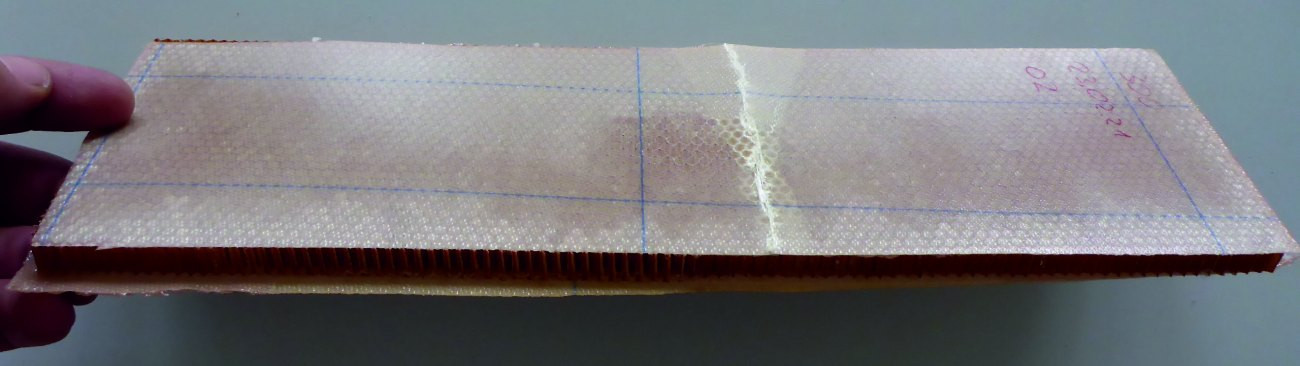
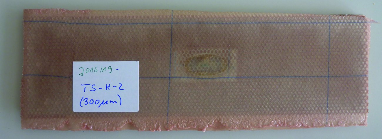
Fig. 24: Sandwich sample with oval RFID tag embedded in the center (top), damage pattern of sample H-2 (bottom)
Further samples were then produced, e.g. also with RFID tags with an oval outer contour, which were then embedded in the middle of the sandwich structures (Fig. 24 above).
Some of the measurements were carried out with the RFID reader inserted so that the functionality of the RFID tag could be constantly monitored. The damage patterns were correspondingly pronounced(Fig. 24 below). The metallographic preparation of the RFID tag of sample H-2 with subsequent light and dark-field microscopy showed that the joints of the RFD tag had not been damaged despite the breakage of the sandwich sample(Fig. 25).
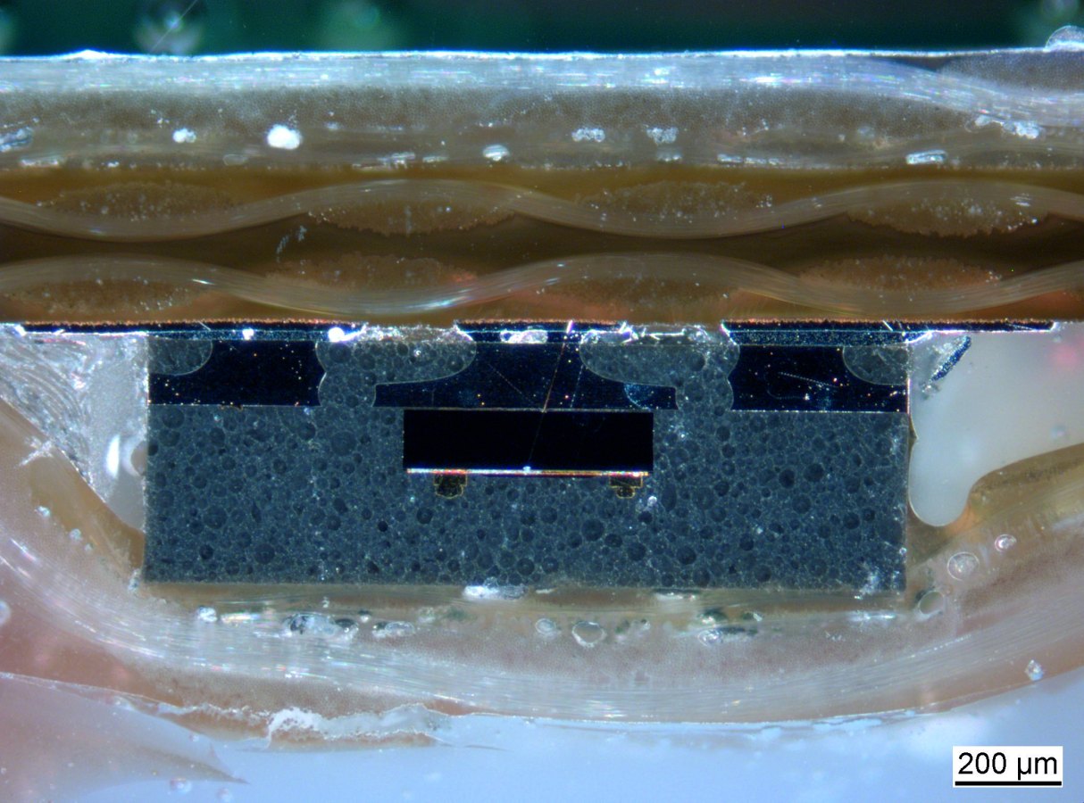
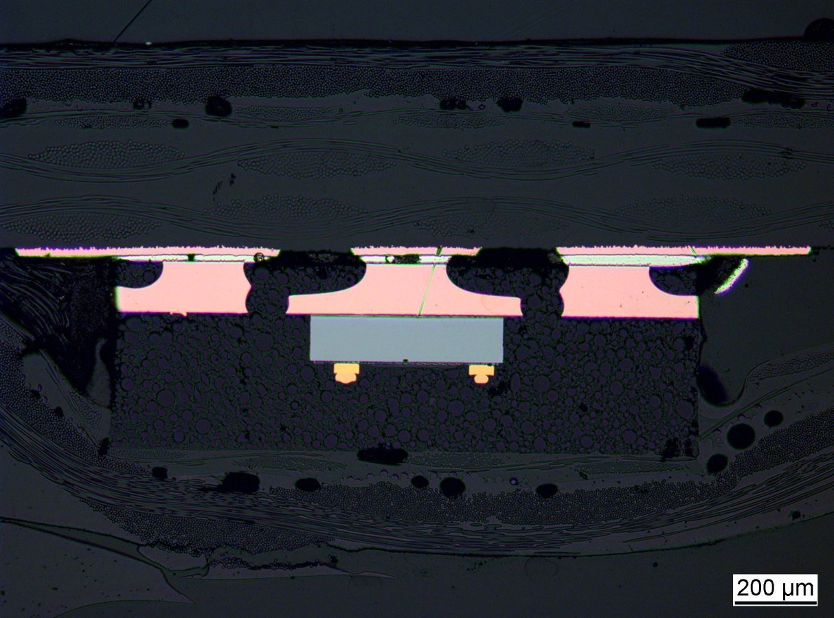
Fig. 25: Light microscope images of the metallographic section of the RFID chip
 Fig. 26: Protective coating and dummy connector as preparation for coatingIn addition tothe tests with increasing static load until failure of the sample, dynamic load cycling tests were carried out. The maximum load for these dynamic load cycles was derived from the failure loads of the static tests and set at 70 % of this failure load. For example, 10,000 load cycles with a maximum load of approx. 600 N were carried out on a specific sample. One load cycle lasted approx. 35 s. This resulted in a maximum deflection of 9.7 mm. A failure of the RFID tag could not be detected. As a qualitative summary of all static and dynamic tests on samples with RFID tags, the following can be stated:
- All failure loads were in comparable ranges
- Tests in which the RFID tag was embedded downwards in the sample during the load (tensile load) achieved slightly lower failure loads than those in which the RFID tag was embedded on top (compressive load)
- All RFID chips were still functional after failure of the sample
- The structural failure of the samples was shown by the detachment of the adhesive of the cover layer at different points with breakage of the sample
- In the dynamic tests with approx. 70 % of the failure load, there was no structural failure of the samples. All RFID tags were functional during the entire 10,000 load cycles.
These results provided a good basis for the next step with the embedding of more complex electronics. A Raspberry Pi Zero mini PC was chosen as the vehicle for this, which represents a small, low-power computing unit with a minimal overall height and can be used via a few connections (HDMI, USB and SD card for software).
 Fig. 27: Raspberry Pi Zero with additively applied protectionThetopographically jagged surface of the assembly, consisting of various materials, appeared to be critical for the bonding of the phenolic resin structures of the top layer and honeycomb fabric, so that prior coating of the assembly seemed sensible. To protect the connectors to be used later from the penetration of the coating material, a protective coating was applied or dummy connectors were inserted into the connection sockets before the actual coating(Fig. 26).
It also had to be taken into account that the coating material would later be exposed to the process conditions of sandwich production. Initial trials with a promising sheet-mold material (originally from wafer-level molding) were not successful. Finally, a special additive technology was used, with which a complete equalization of the topology of the electronic assembly could be achieved(Fig. 27).
Various embedding scenarios were realized with this configuration. Firstly, the Raspberry Pi was embedded in such a way that the connectors were accessible at the edge of the sandwich component. On the other hand, corresponding cables were plugged into the connections of the Raspberry Pi and embedded. An RFID tag was also embedded in both variants(Fig. 28).
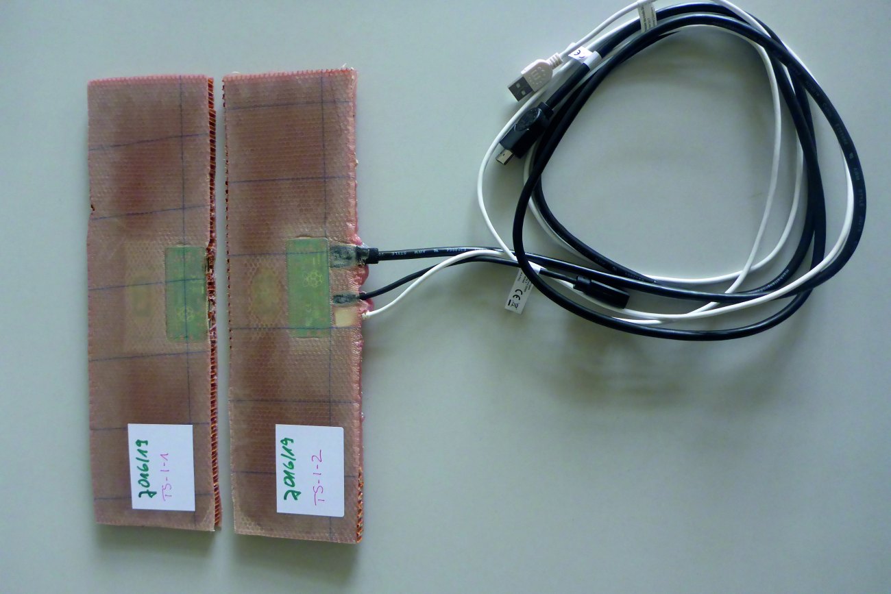
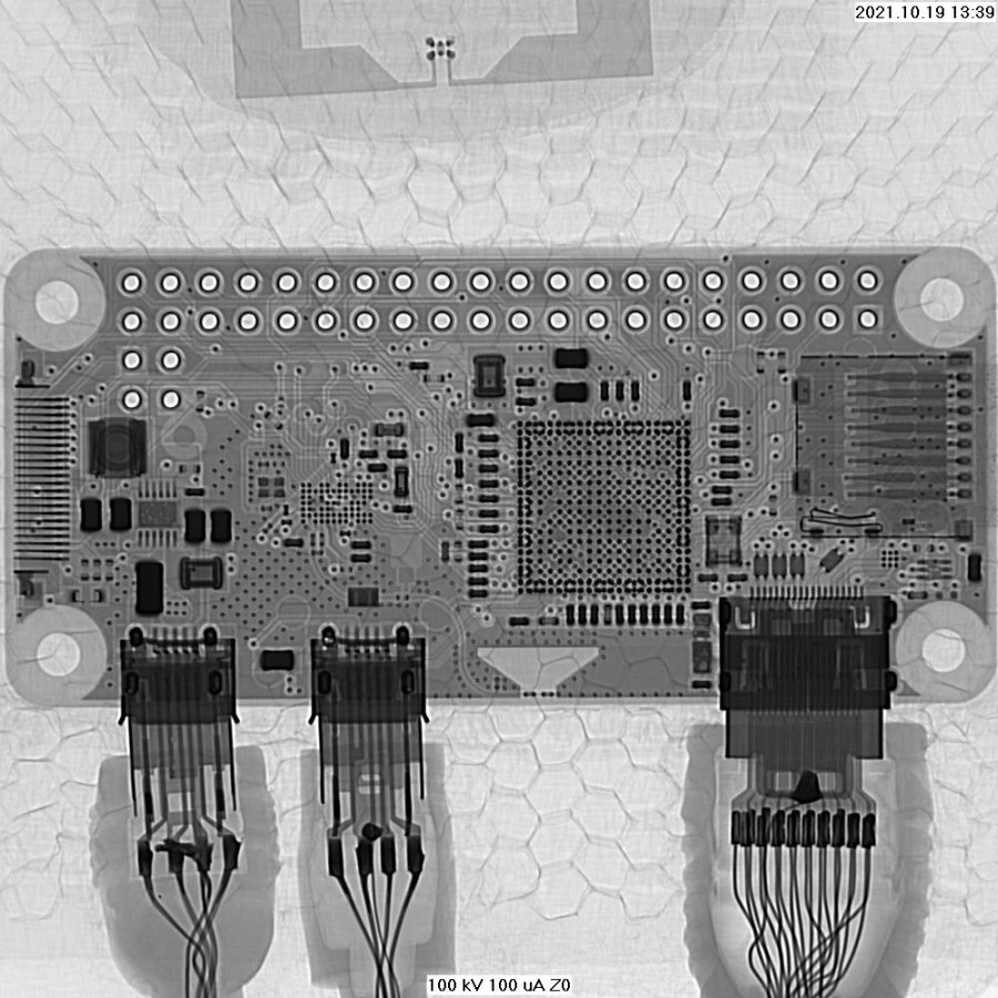
Fig. 28: Sandwich components with two arrangement variants of the Raspberry Pi (left), X-ray image of the variant with connected cables
These samples were to be subjected to dynamic tests. The first corresponding test was based on a maximum load of 600 N. The Raspberry Pi was aligned downwards in the sandwich structure during the load change. A maximum deflection of 9.9 mm was achieved. However, structural failure of the specimen occurred after just 8 cycles. The greater stiffness of the encased electronic module obviously weakened the sandwich component against the bending load. The fracture in the top layer occurred on the upper side of the sample, i.e. opposite the embedded electronics(Fig. 29). The additionally embedded RFID tag was still functional.
 Fig. 29: Sample with structural damage after 8 cycles
The applied load and the deflection achieved by it were far above the permissible values, which is why they could be reduced without reducing the significance of the results in the interest of a higher number of cycles. For the test with the second sample, the maximum load was reduced to 450 N. The maximum deflection achieved was 7.1 mm. So far, more than 500 cycles have been completed without any damage occurring.
Concept for possible panel connections
An important point to be solved for the actual application of embedded electronic modules in sandwich components is the assembly and maintenance-friendly connection of individual lightweight components to each other. Figure 30 shows a systematization of the connection options. Wireless connections to the embedded electronics, as practiced here with the RFID tags, are well suited for connecting users' mobile devices or for contactless radio identification of the sandwich components.
 Fig. 30: Classification of connection types for electronic modules in sandwich components
Wired electrical or optical connections, on the other hand, are suitable for connecting sandwich components to each other and for implementing bus systems. They are less susceptible to interference than wireless connections and allow the transmission of larger amounts of energy. However, they require exposed connecting elements during embedding. The two variants chosen for embedding the Raspberry Pi should also be considered in this sense, i.e. on the one hand with plug-in connections of the embedded electronics located at the edge of the sandwich component and on the other hand with electronics embedded in the middle and separately led out connections. For the latter, a wide range of variants with cables, flex and rigid-flex substrates can be imagined. Extensive research work still needs to be carried out in this regard in order to take into account all relevant requirements for approval in the aerospace sector.
Summary and outlook
The 'Component 4.0' project has brought together and bundled expertise from the fields of lightweight construction for aircraft cabin interiors and electronics technology. The feasibility in principle of embedding simple and more complex electronic modules in sandwich components was demonstrated. The adaptation between approved materials for sandwich components and the electronic modules is possible.
The typical loads that may act on cabin components can be classified as unproblematic and easily tolerated by the internal electronics. Instead, the potential weakening of the structural component due to the introduced "disturbance variable" electronic module must be taken into account. Static and dynamic load tests have shown that this weakening of the structural component is easily manageable. A simple structure was modeled and simulated using FEM. The agreement with experimentally determined data was very good. The simulation also shows that simple geometric adjustments in the sandwich structure increase the resistance despite the embedded electronics.
For the embedded electronics, a conscious decision was made to use proven standard technologies in assembly and connection technology. These should be able to pass the demanding avionics-specific approval procedures for components more easily than current high-end technologies, e.g. the additive construction of electronic components.
Based on these initial investigations, potential follow-up projects can work together with industrial partners to develop practical applications.
Acknowledgements
The research project 'Functionally integrated sandwich components for the aircraft cabin as a prerequisite for Industry 4.0 and innovative operational and MRO processes' (acronym 'Bauteil 4.0') was funded by the Federal Ministry for Economic Affairs and Energy (BMWi) by decision of the German Bundestag within the aviation research program LuFo V-3 under the funding codes FKZ 20X1727A, 20X1727B and 20X1727D.
The project consortium IMA Materialforschung und Anwendungstechnik GmbH Dresden, Dresden University of Technology (Center for Microtechnical Production) and Hamburg University of Technology (Institute of Aircraft Cabin Systems) would like to thank external partners, in particular 3D ICOM GmbH & Co. KG, Hamburg and Großenhain, for funding this project and for their support.
References
Image source: Audi - Virtual Cockpit in the Audi TT: https://www.autoevolution.com/news/virtual-cockpit-in-new-audi-tt-changes-the-world-of-connectivity-video-84372.html# (accessed on 10.11.2021)
Image source: Bundesverband der deutschen Luft- und Raumfahrtindustrie; Video by Airbus & BDLI for the Aircraft Interiors Expo 2012 "AIX 2012 Imagine Innovations Flying Tomorrow ": https://www.youtube.com/watch?v=WNpVHj8WiM8 (accessed on 16.01.2022)
Image source: https://mediacentre.airbus.com/mediacentre/media?mediaTitle=title_MAVERIC+CABIN&mediaId=516505 (accessed on 24.01.2022)
Image source: Produced by George William Herbert, CC BY-SA 2.5, https://commons.wikimedia.org/w/index.php?curid=1197462
ASTM D7249: Standard Test Method for Facing Properties of Sandwich Constructions by Long Beam Flexure
Datasheet available at: https://www.gurit.com/en/our-business/composite-materials/prepregs/aerospace/ph-600--pf-800
Datasheet available at: https://www.schuetz-composites.net/de/honeycombs/cormaster-c1/
Ralf Seemann, A Virtual Testing Approach for Honeycomb Sandwich Panel Joints in Aircraft Interior, Springer Verlag, 2020.
