The electronics of the future are unthinkable without two-dimensional materials. However, their unique properties make doping them with foreign atoms difficult. However, this step is necessary in order to precisely adjust the electrical conductivity and transform the material into a p-type or n-type semiconductor.
A team from the Helmholtz-Zentrum Dresden-Rossendorf (HZDR) and Chemnitz University of Technology has now achieved a breakthrough. A capping layer used by them makes it possible to process the new materials using the processes already established for conventional semiconductors. This is a major step on the way from the laboratory to industrial production.
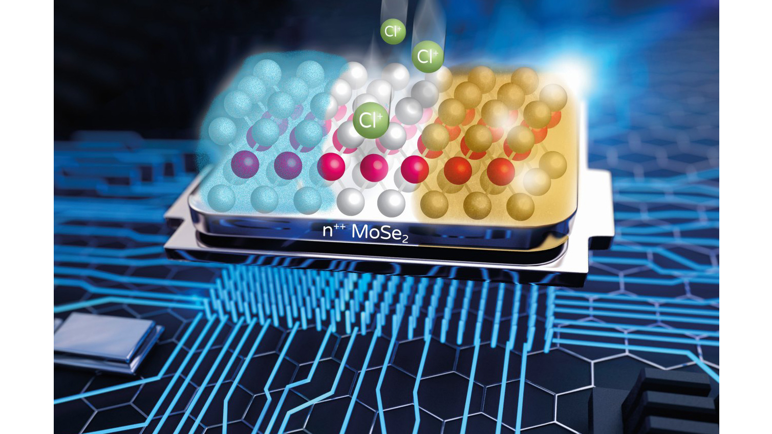
Alternatives to the silicon commonly used today are ultra-thin, two-dimensional materials such as graphene or transition metal dichalcogenides. They are only a few atomic layers thick. In order for the new 2D materials to function as electronic components, their internal properties must be modified by doping. Ion implantation is difficult with these materials, which are only a few atomic layers thick, because the ions from the beam must stop precisely in the few atomic layers that make up the material. The team at the HZDR has therefore provided the new materials with a special top layer. The structure of this layer makes it possible to control the doping process very precisely.
