Fraunhofer at electronica 2022 The Fraunhofer-Gesellschaft was also represented with a joint stand at electronica in Munich from November 15-18, 2022. Current research topics and the resulting products were presented in a press tour on November 16. Thin-film and plasma technology processes are used in many of these applications.
Energy harvesting
Minimal vibrations, temperature differences or light can be used to generate electricity for small electronic systems. The industrial "Internet of Things" consists of millions of sensors, each of which requires only small amounts of energy, but which are very energy-intensive in total. With energy harvesting technologies, these sensors can draw energy from heat, light or vibration and thus operate completely autonomously, without any cables or batteries. The Fraunhofer Institute for Integrated Circuits IIS showed, among other things, a NarrowBand IoT module that transmits supply data in a 5G network (Fig. 1). This paves the way not only for energy self-sufficient LPWANs, but also for other wireless systems with higher energy consumption and other functionalities such as bidirectional communication and operation in a public network.
Virtual prototyping
The Fraunhofer Institute for Integrated Circuits IIS, Adaptive Systems Engineering branch EAS, also demonstrated how virtual prototyping can be used to detect errors and problems in complex control electronics at an early stage based on simulation, shorten development times and significantly reduce costs.
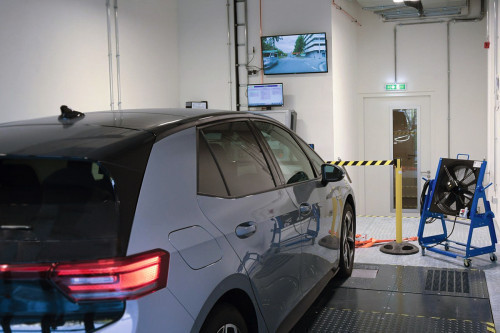
Development cycles in microelectronics are much more complex than in traditional mechanical engineering. For application-specific integrated circuits, so-called ASICs, and other embedded systems, lead times of six months and longer are not uncommon. Virtual prototyping is used to shorten processes. Parts of the product development chain are supported by simulations. By using virtual models, intensive software tests can begin long before the hardware is available. In addition, a significant reduction in time and costs can be achieved, which, for example, saves the real model in the automotive sector many millions of kilometers driven (Fig. 2).
Novel AR assistance system for industrial use
In the future, factories will have to manufacture individual products even more flexibly than today and achieve greater efficiency, in a short time, at low cost and with the highest quality. Modern AR (augmented reality) assistance systems will provide employees with the best possible support and integrate them into production and service processes. This makes it possible to improve working conditions and production processes and also opens up completely new business models and services.
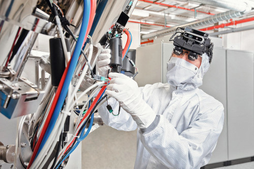
The Fraunhofer Institute for Organic Electronics, Electron Beam and Plasma Technology FEP presented the prototype of an AR assistance system for industrial production in electronics and aircraft construction from the secureAR project, which aims to ensure improved working and production processes for factories of the future (Fig. 3). The modular system integrated into a bump cap comprises OLED microdisplays and additional cameras. This allows operating instructions or information to be displayed to remote persons. The sensors and interfaces can be expanded and the container-based server structure enables controlled data storage.
The use of tiny OLED microdisplays, which consume hardly any power, has resulted in a lightweight, ergonomic system that can be used both binocularly and monocularly.
Laser-based silicon crystallization for monolithic integration in MEMS sensors
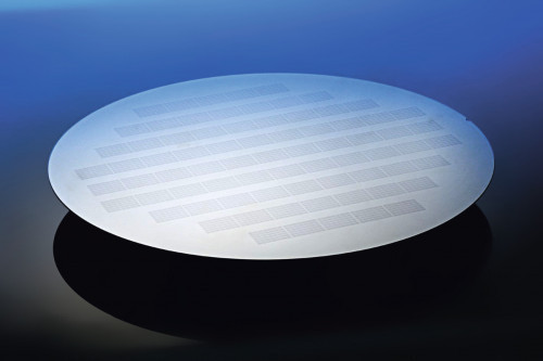
 Fig. 4: Gentle high-temperature crystallization: Together with Fraunhofer ISIT and IST, Fraunhofer ILT has developed a selective, laser-based crystallization process for MEMS sensor units (Photo: Fraunhofer ILT, Aachen)
Micro-electromechanical systems (MEMS) have proven themselves as sensors in smart cars, cell phones and mini insulin pumps, among other things: To make them even more powerful in the future, Fraunhofer researchers have developed a CMOS-compatible coating and laser crystallization process (Fig. 4).
In contrast to conventional methods, this process eliminates the need for wires and solder joints, which can significantly reduce component size and increase sensor performance in the future. This laser-based process is used as an alternative to conventional joining techniques and makes it possible to build MEMS sensors made of crystalline silicon directly (monolithically) on the temperature-sensitive circuits. The researchers are taking advantage of the fact that amorphous silicon layers can already be produced at low temperatures below 450 °C on the circuit-carrying wafer at high deposition rates. The laser not only crystallizes this silicon layer locally selectively and very quickly, but also activates the dopants it contains, thereby ensuring suitable electrical conductivity. The sensitive electronics on the underlying substrate are not damaged and mechanical stresses in the layer material can be minimized. The sensor units are then exposed using conventional microelectronic manufacturing processes.
The newly developed process reduces the electrical resistance of the silicon layers by more than four orders of magnitude below a value of 0.05 Ω*cm. With a layer thickness of 10 µm, this corresponds to a sheet resistance of 50 Ω/sq. MEMS sensors with typical finger structures for a capacitive acceleration sensor could be produced from these layers. Details of the project and its results were presented by Fraunhofer.
Sensor and actuator-related signal preprocessing with AI
The Fraunhofer Institute for Photonic Microsystems IPMS combines the latest hardware in microsensor and actuator technology with artificial intelligence. Digital helpers such as smart apps or cars that think for themselves are already firmly integrated into everyday life. At present, however, the data is usually processed on large, external servers.
Embedded artificial intelligence (edge AI) is set to change this and enable data and algorithms to be processed directly on the end device. However, the performance of edge AI, especially in small devices, is currently still very limited. IPMS is therefore researching innovative solutions to integrate machine learning algorithms into everyday devices. A demonstrator set-up at electronica showed an example of signal pre-processing with sensors and actuators (Fig. 6). The areas of application for the sensors and actuators used include spectrometers, ISFET sensors and ultrasound imaging (for condition monitoring, gesture control or environment recognition in cobots).
Smart LIDAR sensor
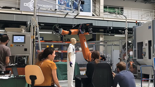
 Fig. 5: Acquisition of initial application-specific training data for the system's AI (Photo: Fraunhofer)
In the Fraunhofer lighthouse project NeurOSmart, five Fraunhofer Institutes (ISIT, IPMS, IMS, IWU, IAIS) are jointly researching a particularly energy-efficient and intelligent distance sensor (LIDAR) for the next generation of autonomous systems. At electronica, they presented the anticipated sensor system and the hybrid, neuromorphic data processing pipeline (Fig. 5). The current trend for complex, demanding applications, such as autonomous driving, is towards mobile supercomputers with significantly higher energy consumption. For mobile systems in particular, this is leading to shorter operating times or ranges and, according to current forecasts, will even reach the limits of global energy generation in the coming decades. To counteract this escalation, the Fraunhofer researchers involved in NeurOSmart are focusing on decentralized intelligence that is tailored to the respective sensor and on new approaches to energy-efficient data processing.
The basic idea of the project is to integrate data processing directly into the sensor as far as possible and to become as energy-efficient as possible by using coordinated components. The desired result is a distance sensor (LiDAR) that detects and classifies objects based on individual pixels in a field of view of 90° x 90° at working distances of up to 12 meters. All this in real time with refresh rates of over 20 Hz and with an energy consumption of just a few 10 W. This system can therefore be used as a safety system for collaboration between humans and industrial robots and, in future, also for mobile applications.


