The advantage of metallizing plastics lies in the possibility of combining different properties of the individual materials to create functional components. Plastics are light and flexible, and the metallic layer opens up new possibilities for modifying the properties of the plastic. In this context, the main aim of the investigations carried out here was to develop two processes for external currentless metallization using palladium pickling without exposing the plastic surfaces to a chromium-sulphuric acid pickling process.
The nucleation was carried out on the one hand by treatment using atmospheric pressure plasma (APPCVD) and on the other hand by a purely wet-chemical process. Adhesion tests and imaging analyses of the layers produced show that both APPCVD and wet-chemical pickling are alternatives to conventional metallization of plastic surfaces
1 Introduction
The metallization of plastics has become an important process in today's world. It opens up the possibility of combining the properties of plastics and metals. As a base material, plastic is lightweight and resistant to corrosion. Plastic components are also lightweight and inexpensive to manufacture. The applied metallic layer ensures, for example, that the plastic surface is electrically conductive, which allows the use of such metallized plastic components in various areas [1, 13]. Chemical metal deposition can be used to metallize plastic surfaces. Processes for this are immersion or contact processes, in particular the electroless nickel process. In the latter case, the plastic surface is coated without external current. This makes it possible to apply a conformal coating with tolerances of ± 2 to ± 3 µm in layer thickness ranges from 8 µm to 80 µm [2]. The aim of the investigations carried out here was to develop new methods for the nucleation and metallization of plastic surfaces. In industry, the sterilization of plastic samples is initiated by pickling with chromium-sulfuric acid [3]. This procedure was not used here and instead the atmospheric pressure plasma deposition process (APPCVD) was used to deposit palladium nuclei on the plastic surfaces. Furthermore, a completely wet-chemical nucleation process was chosen to apply palladium nuclei to the surface of the plastic. In addition, the electroless nickel process was carried out with two different electrolytes. The focus of these investigations was on the production of homogeneous nickel layers with high adhesion strength on the plastic substrate without having to pickle the substrates with chromium-sulphuric acid beforehand.
2 Material and methods
2.1 Process 1 - APPCVD
![Abb. 1: Schematischer Aufbau einer APPCVD-Plasmaanlage während der Beschichtung [4]](/images/stories/Abo-2020-12/thumbnails/thumbnails/GT12-20-61.jpeg "Abb. 1: Schematischer Aufbau einer APPCVD-Plasmaanlage während der Beschichtung [4]") Fig. 1: Schematic diagram of an APPCVD plasma system during coating [4]A special process of chemical vapor deposition is the deposition of thin films by plasma under atmospheric pressure (Fig. 1).
Fig. 1: Schematic diagram of an APPCVD plasma system during coating [4]A special process of chemical vapor deposition is the deposition of thin films by plasma under atmospheric pressure (Fig. 1).
A chemical precursor can influence the functional properties of the coating. The feed points of the precursor also have a decisive influence on the coating properties [5]. In the atmospheric plasma coating process, a distinction is made between direct and remote operation, depending on whether the precursor is introduced into the active plasma zone or not. The precursor is then chemically converted in the plasma and reaction products are transported to the surface of the substrate. As a result, functional layer thicknesses of up to around 200 nm are possible; the roughness of the respective layer can be controlled and is in the range of a few nanometers. At Innovent, SiOx, TiOx and SnOx are currently cultivated as layer systems, and composite layers loaded with active substances are also possible [5-9]. In contrast to the APPCVD composite layers produced to date, the deposition of a SiOx matrix layer was dispensed with in these investigations and only the added palladium nanoparticles were used as a functional coating [4].
An atmospheric plasma system "Plasma T-Spot" (Tigres GmbH, Marschacht) was used in these investigations. The discharge takes place between a centrally arranged high-performance ceramic electrode and the nozzle serving as a counter electrode. Due to the combination of the nozzle geometry and the electric current flowing through the nozzle, two areas of this discharge are formed. The current filaments of the primary plasma can be seen directly at the nozzle. The second area of the plasma discharge is the secondary plasma without filaments [10, 11]. This plasma system can be used for both conductive and non-conductive materials. The adjustable power range is between 250-500 watts [11, 12]. Two coating modes are realized using the T-spot. In direct mode, the palladium precursor is added upstream of the plasma, while in remote mode the precursor is added via an external injection system outside the plasma nozzle. The precursor is dosed via an ISMATEC ISM597D peristaltic pump (Cole-Parmer GmbH, Wertheim) and a dosing nozzle, which feed the precursor into an aerosol spray system. There it is converted into an aerosol with the process gas air and transported to the plasma nozzle. The palladium precursor used is made up of the following components:
- Palladium (II) chloride
- 35% fuming hydrochloric acid
- anhydrous isopropanol
Palladium nucleation is carried out on polyamide 6, polyetherimide flat substrates and on silicon wafers to analyze the palladium particles. Due to the different substrates, both the travel speed and the duration of the coating were varied.
2.2 Process 2 - Chemical nucleation
The second method carried out here for the metallization of plastics is wet chemical nucleation with tin chloride and palladium chloride with subsequent chemical nickel plating in a slow-growing electrolyte. The plastic samples are cleaned before germination and pre-activated with a low-pressure plasma (2.45 GHz microwave plasma, working pressure approx. 1 mbar, air as process gas, 16 s treatment time) in order to functionalize the surface. This process is essential for good bonding of the palladium nuclei and thus for an adhesive bond of the nickel layer. After preactivation, the samples undergo a series of germination and rinsing cycles. The stannous chloride bath acts as a pickling agent on the plastic. The palladium nuclei for the subsequent nickel plating are applied to the surface by the palladium chloride bath. The various rinsing passes are intended to prevent contamination of the individual baths and at the same time improve the adhesion of the palladium particles due to the temperature differences. After germination, the samples are dried and can then be nickel-plated in the electrolyte.
2.3 Electroless nickel plating process
The electrolyte HSO Evolution L (HSO Herbert Schmidt GmbH & Co. KG, Solingen) is used for process 1 of electroless nickel plating. The samples are nickel-plated at 78 °C for approx. 10 minutes. Only this short plating time is required as it is a fast-depositing electrolyte. A slow-depositing electrolyte is used for process 2. The advantage of this electrolyte is that it can be operated at very low process temperatures (approx. 40 °C) and is therefore also suitable for thermally sensitive substrates such as plastics. In addition, the lower deposition rate of the electrolyte ensures better bonding to the substrate and leads to low residual stresses in the layer. The electroless nickel plating time for process 2 was approx. 35 minutes.
2.4 Surface analysis
Various methods were used to analyze the nickel layers produced. A SUPRA 55 VP scanning electron microscope (Carl Zeiss NTS GmbH, Oberkochen) was used to obtain detailed images of the coating surface and the cross-section of the samples. In addition, the resulting palladium particles are analyzed for their bonding state using the AXIS ULTRA DLD X-ray photoelectron spectrometer (Kratos Analytical Ltd, Manchester, UK). The electrical resistance of the metallized plastics was measured using the 4-point measuring device SD-600 (Nagy Messsysteme GmbH, Gäufelden, Germany). The measuring device determines the sheet resistance of the layers by specifying the sample area.
2.5 Shear strength
To determine the adhesive strength, a shear test was carried out in accordance with DIN EN ISO 22632. The testing machine was a tension-compression machine with the standard testing tool. The metallized samples were bonded using a 3M Scotch-Weld DP 460 - 2-component epoxy resin adhesive (3M Deutschland GmbH, Neuss) with a steel test stamp (diameter 5 mm). The stamps were later sheared off by applying force and the shear strength was determined on the basis of the adhesive surface. Furthermore, the fracture point was visually inspected after the shear test in order to make a statement about the fracture mechanism.
3 Results and discussion
3.1 Particle analysis
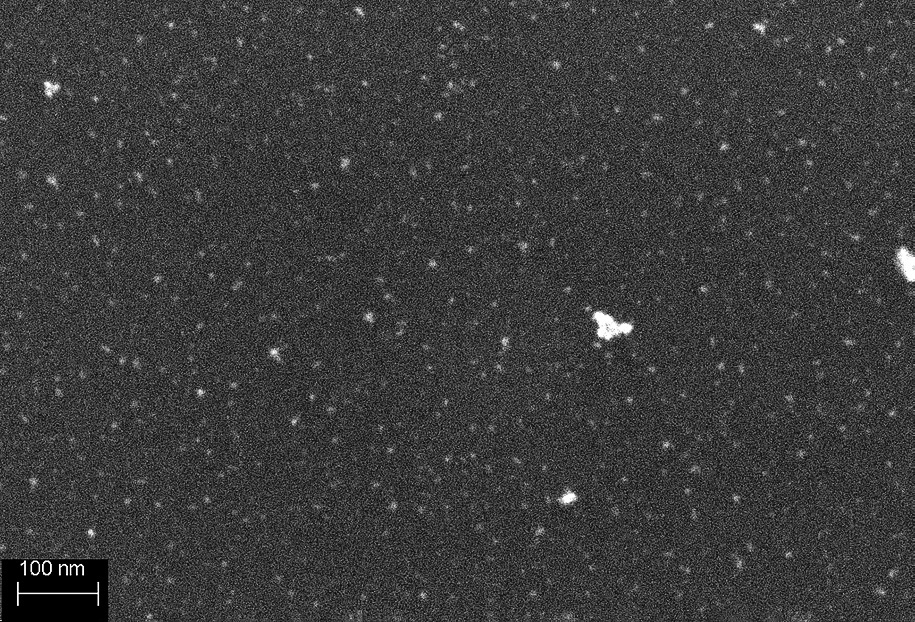
The analysis of the palladium particles provides important information about the different modes of atmospheric pressure plasma nucleation. To what extent do the shape of the particles and their size change when they are applied to the substrate surface in direct or remote mode? Fig. 2 shows the particles after process 1 (APPCVD germination).
 und remote-Modus (rechts) Bekeimung") Fig. 2: SEM image of the palladium particles on silicon wafers after direct-mode (left) and remote-mode (right) nucleation
Fig. 2: SEM image of the palladium particles on silicon wafers after direct-mode (left) and remote-mode (right) nucleation
The palladium particles in direct mode are significantly larger than the particles in remote mode and have a cluster-shaped structure. The remote particles have a spherical structure and are much finer than in direct mode.
Figure 3 shows the palladium particles after process 2 (wet chemical germination). The palladium particles after chemical nucleation are very small and only occasionally form cluster-like structures. An additional magnification of the particles reveals even finer particles (Fig. 3 right).
 Fig. 3: SEM image of the palladium particles on silicon wafers after chemical nucleation
Corresponding XPS measurements were carried out on the germinated surfaces for both germination processes. In process 1, a difference in the bonding state of the palladium particles was observed. While in direct mode all of the palladium (1.68 at%) was increasingly detected as palladium oxide on the plastic surface, in remote mode up to 50% of the palladium present (1.49 at%) was detected as metallic palladium. The proportion of metallic palladium is crucial for good bonding of the nickel layer. In process 2, no statement could be made about the bonding state, as the total amount of palladium (0.59 at%) on the surface was too low.
Due to the generally smaller particles from process 2, adherent, homogeneous nickel layers can grow on smooth plastic surfaces. The larger particles from process 1 only allow the growth of such a nickel layer on plastic samples previously roughened by sandblasting (abrasive: aluminum oxide, grain size 130 µm). This can be explained by the van der Waals forces that act between the particles and the surface. Smaller particles adhere better to smooth surfaces than larger particles. As a result, only a very inhomogeneous layer grew on smooth samples after APPCVD germination, which detached under low mechanical stress.
3.2 Layer analysis
The topography of the nickel layers produced in both processes can be easily visualized using SEM examinations. In addition, cross-sections of the samples were made and the layer thicknesses measured in the SEM. Figures 4 and 5 show the different structures of the nickel layers after processes 1 and 2. Figure 6 shows a cross-section of the layer after process 1.
 Fig. 4: SEM image of the surface of a nickel layer after process 1
 Fig. 5: SEM image of the surface of a nickel layer after process 2
 Fig. 6: SEM image of the cross-section of a nickel layer after process 1
The nickel surface after APPCVD pickling (process 1) shows roundish shapes with small cracks. After wet-chemical nucleation (process 2), finer structures can be seen in the nickel layer. The nickel layer after process 2 also appears smoother than the nickel layer after process 1. This observation can also be attributed to the different palladium particle sizes. Smaller particles result in a smoother nickel layer, while the larger particles increase the roughness of the samples. As an example, sandblasted plastic samples for process 1 resulted in square center roughness values (Rq) of approx. 5 µm, while they were only approx. 3 µm for process 2.
The layer thickness after process 1 was determined with the SEM and averages 3 µm, with a sheet resistance of approx. 0.5 Ω. The coating thickness after process 2 was determined by means of paint masking with subsequent profilometry. Here, a coating thickness of approx. 2 µm was measured and corresponding sheet resistance of 2 Ω. Higher layer thicknesses can be realized with the slow-depositing electrolyte by further extending the coating time.
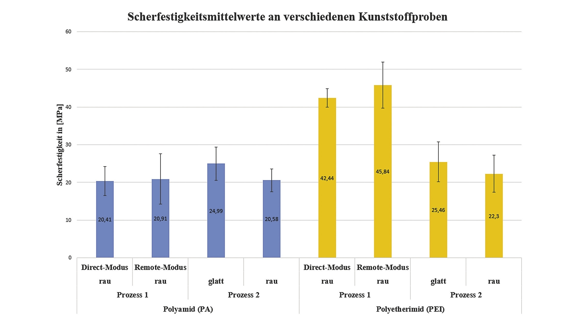
3.3 Shear strength
Figure 7 shows the shear strength results after processes 1 and 2. The diagram shows that the nickel coatings on polyetherimide tend to have a higher shear strength than the nickel coatings on polyamide. However, both processes and plastics resulted in an adhesion failure between the stamp and the adhesive. For this reason, the shear strengths of the nickel layers are higher. Process 2 has similar shear strength values for polyamide and polyetherimide. A shear strength of approx. 45 MPa was achieved by the polyetherimide layers, which were previously roughened and seeded using the APPCVD process.
4 Summary
It was shown that both the APPCVD process and the chemical process can be used as an alternative to a chromium-sulfuric acid-based pretreatment of plastic surfaces for the nucleation of plastic surfaces. By using different electrolytes, it was possible to deposit homogeneous, adhesive nickel layers on roughened and smooth polyamide 6 and polyetherimide surfaces. The layer thicknesses obtained were also comparable.
The advantages of APPCVD nucleation lie in its rapid application, a lower number of bath and dipping processes and the high layer thickness that can be achieved within a short time. However, this method has so far only been able to achieve satisfactory coating results on roughened substrate surfaces. The method is still primarily suitable for flat substrates. In the future, the metallization of simple geometries (e.g. rotationally symmetrical components, components without undercuts) will also be targeted with appropriate technical adjustments to the system.
The advantages of chemical nucleation lie in the low layer stresses that build up during slow metallization and the suitability of the coating method for more complex 3D geometries. This method also makes it possible to apply a homogeneous, adhesive nickel layer to very smooth substrates due to the small palladium particles. However, this method is more time-consuming and produces slightly thinner layers compared to the APPCVD process.
Future investigations will focus on modifying the process variants so that, for example, smooth plastic surfaces can also be seeded using APPCVD. In this respect, the remote mode offers the option of creating smaller palladium particles. Work should also be done on increasing the layer thickness in the slow-growing electrolyte.
5 Acknowledgments
The authors would like to thank A. Henning for the scanning electron micrographs of the layers produced and for his support with the chemical nucleation using tin and palladium chloride. We would also like to thank M. Goetjes for the profilometric investigations of the samples produced. Special thanks go to B. Kretzschmar for the measurement and evaluation of the XPS data for the analysis of the palladium particles. Parts of this work were financially supported by the BMWi under grant number ZF4028635VS9.
Literature
[1] D. Rathmann: Plastic electroplating, In: Chemie in unserer Zeit, Vol. 15, No. 6, 1981, pp. 201-207, doi:10.1002/ciuz.19810150606
[2] Electroless nickel, https://www.chemie.de/lexikon/Chemisch_Nickel.html, 09.11.2020
[3] Electroless nickel - plastic coating,
http://www.electroless-nickel.de/kunststoff.htm, 09.11.2020
[4] A. Pfuch; J. Schmidt; A. Heft; O. Beier; W. Hering; B. Grünler: Atmospheric pressure plasma coatings as a tool in the technology toolbox for surface functionalization; WOMag 10/2015
[5] A. Pfuch; K. Horn; R. Mix; M. Ramm; A. Heft; A. Schimanski: Direct and remote plasma assisted CVD at atmospheric pressure for the preparation of oxide thin films, in: Jahrbuch Oberflächentechnik vol. 66, 114-124, ed. R. Suchentrunk, Leuze Verlag Bad Saulgau
[6] S. Gerullis; O. Beier; A. Pfuch; B. Grünler: Highly Active Photocatalytic Coatings for Temperature Sensitive
Substrates based on Titanium Oxide and Zinc Oxide prepared by Atmospheric Pressure PECVD and Sol-Gel Deposition, NANOCON 2017 Conference Proceedings,
1st Edition 2018, TANGER Ltd, Ostrava, Czech Republic,
[7] S. Gerullis; L. Pohle; A. Pfuch; O. Beier; B.S.M. Kretzschmar; M. Raugust; E. Rädlein; B. Grünler; A. Schimanski: Structural, electrical and optical properties of SnOx films
deposited by use of atmospheric pressure plasma jet,
Thin Solid Films 649 (2018), 97-105
[8] O. Beier; A. Pfuch; K. Horn; J. Weisser; M. Schnabelrauch;
A. Schimanski: Low Temperature Deposition of Antibacterially Active Silicon Oxide Layers Containing Silver Nanoparticles, Prepared by Atmospheric Pressure Plasma Chemical Vapor Deposition, Plasma Processes and Polymers, Volume 10, Issue 1, 2013, 77-87
[9] S. Gerullis; A. Pfuch; S. Spange; F. Kettner; K. Plaschkies;
B. Küzün; P.V. Kosmachev; G.G. Volokitin; B. Grünler:
Thin antimicrobial silver, copper or zinc containing SiOx films on wood polymer composites (WPC) applied by atmospheric pressure plasma chemical vapor deposition (APCVD) and sol-gel technology, Eur. J. Wood Prod. 76 (2018), 229
[10] Plasma T-Spot; https://www.tigres-plasma.de/de/oberflaechentechnik/t-spot-technologie/plasma-t-spot; 25.10.2020
[11] Plasma T-Spot S2 series, https://www.wernerwirth.de/fileadmin/content/bilder/ Maschinen/PDF/WW-Datenblatt_Tigres_T-SPOT_S2.pdf; 17.08.2020
[12] Plasma T-Spot S2 series, https://obs.schall-messen.de/Interneteintrag/PDF/e01a614d-afc9-4407-b5b0-
f0c0271bade8.pdf; 17.08.2020
[13] W. Riedel: Functional chemical nickel plating,
Series of publications on electroplating and surface treatment, Eugen G. Leuze Verlag, 1989
