Film type, crystallization and outlook / continued from GT 6/2024 Film thicknesses, deposition rate and morphology
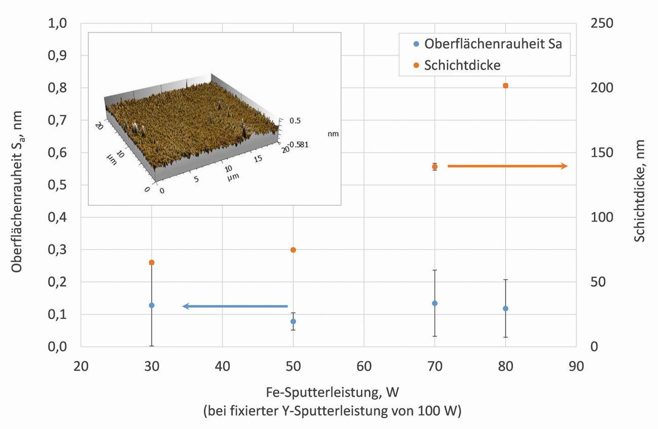
In addition to the spectral ellipsometry described above, the thicknesses of the deposited thin films were mostly determined using tactile measurement methods. This involves moving a scanning needle (stylus measuring tip 2 μm radius / 60 °) over an area covered on the substrate during film production and thus measuring the generated edges with spatial resolution. For our investigations, an Alpha-Step D-600 profilometer (KLA Tencor) was used, which is suitable for recording 3D mappings of the surface and can resolve step heights of up to approx. 1 nm. From the determination of the layer thickness, the layer formation rate for the respective sputter parameter set can then be calculated back via the sputter deposition time. In addition to using the profilometer, the surface topography can also be determined using atomic force microscopy. An aluminum-coated micro-cantilever moves over the surface of the sample, which significantly improves the resolution both vertically and laterally compared to the profilometer. For our measurements, an MFP 3D-Classic (Asylum Research) was used; measurements were taken in tapping mode with a resolution of 256 x 256 pixels at a control frequency of 273.9 kHz. Figure 8 presents results based on topography measurements on untempered YIG layers produced with different iron cathode power. On the one hand, the increase in the layer formation rate with increasing iron cathode power (at a constant yttrium cathode power of 100 W) can be seen very clearly; on the other hand, the arithmetic surface roughness Sa with a very low value of less than 0.2 nm is independent of the layer thickness. The YIG thin films produced can therefore be deposited very smoothly even with film thicknesses in the range of 200 nm, a prerequisite for measuring very good magnetic properties.
 Fig. 8: Results of layer thickness and roughness measurements on YIG layers. The inset shows an AFM topography image of a 200 nm thin YIG film directly after production.
Post-tempering processes, crystallization and magnetic properties
The YIG thin film can only be used in monocrystalline form as a spin waveguide for magnonic applications. For this purpose, the initially amorphously deposited layers must be crystallized. The layers deposited on (111) GGG substrates (Luxium Solutions) and (001) Si substrates (Si-Mat Silicon Materials) were annealed in air at 650 - 850 °C. The activation energy is provided in the form of thermal energy for the crystallization process.
The monocrystalline substrate used additionally reduces the activation energy because crystallization nuclei do not have to form first. This means that the crystallographic orientation of the substrate defines the crystallographic orientation of the crystallized garnet layer.
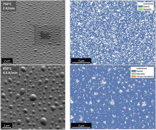
The phase formation in the YIG layers produced was assessed in connection with scanning electron microscopy (SEM) examinations using electron backscatter diffraction (EBSD) measurements. The method is generally very well suited for characterizing crystalline thin films because the depth of information is very low at just a few nanometers. In addition, the roughness of the deposited YIG layers is very low, so that no additional sample preparation is necessary. To carry out the EBSD investigation, only an approx. 2 nm thick carbon layer needs to be applied to the sample surface to ensure the electrical conductivity of the sample. The samples examined here were characterized using an Ultra 55 electron microscope (Carl Zeiss) with an eFlash EBSD detector (Bruker). In addition to characterizing the crystallographic orientation of the actual YIG layer, EBSD can also be used to detect crystalline impurity phases such as Fe2O3 and YFeO3. These phases are formed during crystallization if the actual Y/Fe ratio in the layer deviates from the optimum ratio of 0.6 for YIG. If there is an excess of iron, Fe2O3 is formed in addition to the YIG phase; if there is an excess of yttrium, YFeO3 is precipitated. Fig. 9: SEM image (left) and color-coded EBSD phase mapping (right) for two YIG layers on a GGG substrate, annealed for 1 h at 750 °C (top) and 850 °C (bottom)
The post-annealing processes on the initially amorphous YIG layers on GGG substrates were carried out in a tube furnace (type SR, Gero Hochtemperaturöfen GmbH) between 650 and 850 °C, depending on the temperature. It was shown that crystallization of the YIG layer begins at a temperature of around 750 °C (see colour-coded phase mapping in Fig. 9). At 850 °C, a completely crystallized layer could be detected. Non-indicated areas were caused by unevenness in the samples (see SEM image). For the EBSD diffraction experiment, an angle of 70 ° between the electron beam and the sample surface must be ensured.
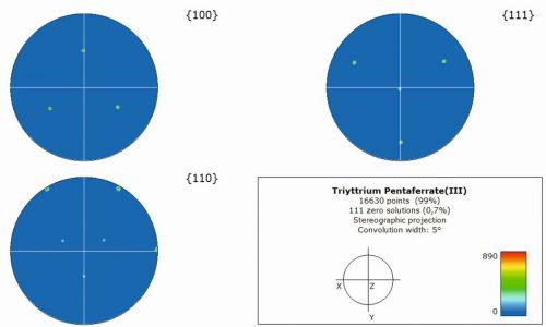
In addition to the detection of the crystallographic phases themselves, the orientation of the crystallized YIG phase could also be described on the basis of the EBSD measurements using pole figures. Such pole figures are one of the most commonly used representations for orientation data. They show the distributions of the selected poles {hkl} taking into account all orientation measurements.
Pole figures thus provide important information about the strength of a texture and also about which texture components are dominant. In the case of the YIG layers produced here, it could be shown that the crystallized YIG layer has the same (111) orientation as the (111) GGG substrate (Fig. 10). The sharpness of the poles reflects the degree of texturization or is a measure of the mosaicity of the single crystal. For a perfect single crystal without lattice defects, the poles would be individual points that are displayed with only one pixel.
 Figure 10: Pole figures of the garnet phase for a YIG layer on a GGG substrate, annealed for 1 h at 850 °C
The magnetic properties of the crystallized YIG layers were characterized by measuring the ferromagnetic resonance frequency (FMR). YIG has the smallest FMR linewidth of all known materials. The linewidth itself is very strongly dependent on the number of lattice defects in the crystal and can be used as a measure of the quality of a YIG crystal or a YIG layer. One of the first YIG layers dc-sputtered and crystallized on GGG showed a line width of the FMR of 9.6 Oe (Fig. 11). This is approximately 10 times the line width of the FMR of a YIG layer deposited on GGG by liquid phase epitaxy according to the state of the art. However, work on rf-sputtered YIG layers with a line width of the FMR of 2-3 Oe is also known in the literature [01]. This shows that there is still potential for improving the FMR properties of dc-sputtered YIG layers through further process optimization.
 Figure 11: FMR properties of a dc-sputtered YIG layer annealed at 850 °C (left) and a YIG layer produced using LPE (right) on a GGG substrate
In initial experiments, YIG layers were also deposited on (100) Si wafers. Using EBSD characterization, it was possible to prove that these layers crystallized polycrystalline due to a lack of epitaxial information of the substrate during the annealing process. In addition, the EBSD-IPF Z map (IPF - inverse pole figure) can be used to determine the crystallographic orientation of the grains in relation to the Z axis (coming out of the plane) (Fig. 12 left). On this basis, it could be shown that the orientation in a grain is not always homogeneous and that in some cases extreme distortions also occur above the grain diameter. This can be explained by the mismatch of the thermal expansion coefficient of YIG and the Si substrate. The occurring grain boundaries and the extreme stresses are the cause of a significantly larger line width of the FMR of 278 Oe (Fig. 12 right).
 Fig. 12: EBSD mapping, here inverse pole figure in z-direction (left) and corresponding FMR measurement (right) for a sputtered YIG layer on (100) - Si
Summary and outlook
In the context of the investigations carried out here, results on the deposition of YIG thin films prepared by dc sputtering were presented. Control of the dc sputtering process via precise monitoring of the discharge voltages and exact determination of the Y/Fe element ratio in the layers and the corresponding optical layer properties allows the production of initially amorphous yttrium-iron-garnet layers with a stoichiometric composition. These layers can be post-crystallized by a subsequent annealing process. The structure of the thin films was elucidated in particular by means of electron backscatter diffraction experiments. Initial results on the magnetic properties of the crystallized YIG layers were presented by means of ferromagnetic resonance measurements. In future experiments, especially the influence of possible buffer layers on the crystalline perfection of the YIG thin films and the magnetic properties will be investigated.
Acknowledgments
The work presented here was supported in part by the Free State of Thuringia with funds from the European Social Fund Plus under the FKZ 2022FGR0008.
Literature
[01]G. Schmidt, C. Hauser, P. Trempler, M. Paleschke, E. Th. Papaioannou; "Ultra Thin Films of Yttrium Iron Garnet with Very Low Damping: A Review", Physica Status Solidi B, 2020, 1900644; https://doi.org/10.1002/pssb.201900644


