Production and layer analysis of YIG layers Introduction
The need for ever more powerful and efficient integrated circuits has led to a continuous increase in the integration density of CMOS components in recent decades. The integration density has doubled approximately every two years (Moore's law). However, this development is increasingly reaching its physical limits. The most modern production technologies allow structure sizes of 5 nm. From structure sizes of 2-3 nm, however, quantum mechanical tunnel currents occur, which will stand in the way of further miniaturization in the coming years. The self-heating of the nanostructures due to the electrical resistance also limits the increase in the clock frequency of the components, as the heat generated can no longer be dissipated by conventional cooling. From today's perspective, the further development of microelectronics can only be achieved through the use of alternative information processing concepts; one of these concepts is based on the use of magnonic components. Transistors that transmit information not via electrons but via spin waves or their quanta, the magnons, generate around 90 % less heat loss compared to conventional semiconductor transistors due to Joule heat transfer. They can also be used up to the THz range.
In recent decades, yttrium iron garnet (Y3Fe2(FeO4)3 or YIG) has emerged as one of the most promising materials for the fabrication of spin waveguides due to its exceptional magnetic damping properties combined with electrical insulation. It has been shown that magnons in YIG can propagate over several centimeters, which is a fundamental requirement for the fabrication of more complex magnonic components. Until now, high-quality YIG layers have been produced using liquid phase epitaxy (LPE) on gadolinium gallium garnet (GGG) wafers. Due to their crystallographic and chemical properties, the GGG substrates are indispensable for carrying out the LPE process, but currently limit the subsequent usable area to 3-4 inches in diameter. A YIG layer on Si wafers would be advantageous for the application of magnonic computing components, as electronic CMOS components are also manufactured on Si wafers. In addition, all known manufacturing processes for YIG layers with excellent attenuation properties are very difficult to scale up for coating larger areas and are only suitable for the production of small sample series for research and development. Significantly more cost-efficient processes for the deposition of large-area thin films for electronic applications are based on the use of plasma processes. In this respect, this article focuses on the production of YIG thin films using dc magnetron sputtering technology and the characterization of these films.
Production of YIG layers
Various methods for the production of YIG thin films are described in the literature. The liquid phase epitaxy LPE, various laser beam evaporation (PLD - pulsed laser deposition) and rf sputtering processes provide YIG layers with the best magnetic properties [01, 02]. Ion beam sputtering, sol-gel processes and CVD coatings are also used. However, these processes generally do not provide the same coating quality as the first-mentioned processes. The Gilbert attenuation α and the ferromagnetic resonance (FMR) curve half-width (FWHM) are used as a measure of the quality of the YIG coatings. For example, YIG layers with a thickness of 1.2 μm and the best attenuation properties to date were produced using PLD processes on GGG substrates [03]. Here, the FMR line width was determined to be 0.9 Oe. This showed that PLD processes can be used to produce YIG coatings with excellent properties. However, the disadvantage of the PLD process is that it cannot be used to coat large areas.
YIG layers only a few nanometers thick can also be produced using LPE in a quality comparable to the PLD process. Dubs et al. were able to produce approx. 100 nm thick YIG layers on GGG substrates with an FMR-FWHM of 1.4 to 1.6 Oe and α = 1.2 - 1.7*10-4 [02]. In later work by the same group, YIG layers up to 11 nm thick could be produced, whereby the excellent damping properties could be maintained [04]. However, LPE processes are limited exclusively to GGG wafers in terms of substrate selection, and the process itself is a batch process that can currently be used to coat wafers up to 3 inches in size. Alternatively, rf sputtering processes using ceramic targets deliver YIG layers with FWHM values that are currently an order of magnitude larger. For example, Bhoi et al. were able to produce approx. 250 nm thick YIG layers on GGG substrates, which had an FMR-FWHM of 40 Oe and an attenuation α of 40.2*10-4 after annealing [05]. Lustikova et al. were also able to produce YIG layers on GGG substrates with a FWHM of 66 Oe and an α of 7*10-4 [06]. However, it should be noted that rf sputtering processes are only suitable for coating larger areas to a limited extent due to their technical characteristics (high-frequency radiation, required shielding, lower power coupling, ceramic targets). In the project presented here, a dc sputtering process was used to produce the YIG layers using two metallic targets (yttrium and iron) at the same time. The dc sputtering process offers several advantages: Firstly, larger areas can be coated with this process in perspective, upscaling is technologically much easier to realize compared to other processes. Secondly, metallic yttrium and iron sputtering targets are relatively inexpensive to procure and the layers do not have to be produced using previously prepared ceramic YIG sputtering targets with the correct stoichiometry, as is currently the case with rf sputtering. Last but not least, the co-sputtering process used here allows independent control of the deposition rates for both metals during sputtering and thus control of the layer stoichiometry while the thin films are still being produced.
Fig. 1: dc co-sputtering process with two metallic targets yttrium (front) and iron (back) 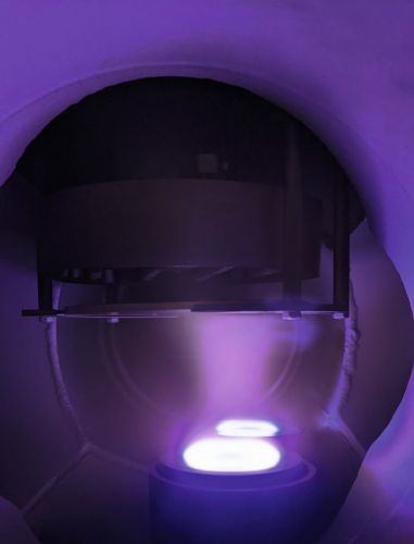 Figure 1 shows a view of the coating system (CreaTec Fischer & Co. GmbH) with the two simultaneously firing sputtering targets yttrium (99.9% purity, Sindlhauser Materials GmbH) and iron (99.95% purity, MaTecK GmbH). In the dc sputter deposition of iron, the thickness of the target must be kept in mind due to the ferromagnetic character of the material. In the investigations presented here, the thickness of the Fe target was around 0.5 mm. This allowed stable operation of the glow discharge during sputtering. The variable process parameters during thin film deposition are primarily the set power of the two cathodes (2" MAG sputtering sources, US Inc.), the working distance of the cathodes to the rotating substrate (here in particular Si and GGG wafers) and the partial pressures of the argon and oxygen during coating. The addition of the reactive gas component oxygen ensures that the oxygen is incorporated into the growing garnet film. The heatable substrate holder is designed to accommodate 4-inch wafers, and an adapter plate can also be used to coat long-cut substrates, for example in slide size, without any problems. In particular, the deposition temperature, which allows the direct production of at least polycrystalline layers, will be included in the investigations in the future. Typical thicknesses of the deposited layers are in the range of around 50 to approx. 200 nm.
Layer analysis
Stoichiometry control using spectral ellipsometry and XRF. The film stoichiometry is mainly controlled by separately adjusting the plasma powers of the two simultaneously burning cathodes. For the investigations, the power applied to the yttrium target was mostly left constant, while the power of the Fe cathode was varied. Accordingly, the absolute element concentrations in the thin films change. The dc power supplies (MDX 1K, Advanced Energy) were operated in power-controlled mode for both targets. As expected, a linear relationship between discharge voltage and applied power was found for the control of the Fe cathode; this relationship is shown in Figure 2. When the Fe target is changed, there is a measurable shift in the discharge voltage due to the associated slight change in the thickness of the target. On the other hand, with regard to the control of the Y cathode, an increasing discharge voltage over time can be recognized, which could be attributed to iron impurities on the yttrium target surface. In this respect, monitoring the electrical process parameters during dc co-sputter deposition is extremely important in order to reproducibly deposit YIG thin films with the required stoichiometry.
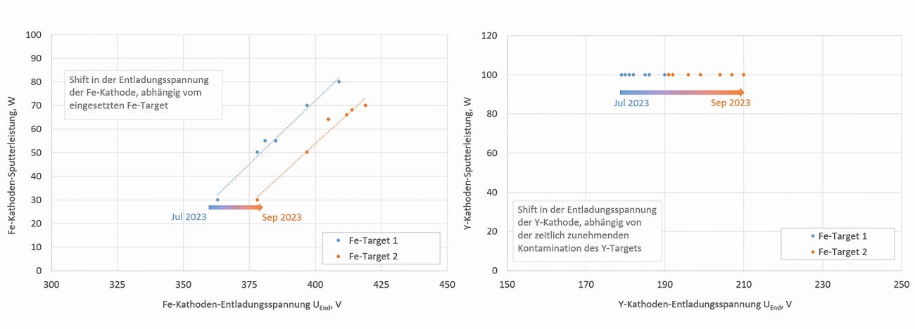 Fig. 2: Discharge voltages during dc co-sputter coating of YIG thin films
Spectral ellipsometry [07, 08] is a non-destructive method for determining the optical properties of transparent thin films. During the measurement, polarized light is directed onto the sample to be measured at a specific angle; the determination of the polarization state of the reflected light forms the basis for the measurement. Since the polarization response depends on the structure and optical properties of the investigated layers deposited on a carrier substrate, ellipsometry can be used to obtain valuable information on the refractive indices, extinction coefficients and layer thicknesses of thin dielectric layers and layer stacks. Spectral ellipsometry is an indirect measurement method. In this respect, a suitable model analysis is required to determine the optical properties. The interpretation of measurement results on the basis of the absolute ellipsometric measurement values Δ and Ψ therefore requires the construction of an optical model. Against this background, the analysis of the ellipsometric data consists of three main parts: the modeling of the dielectric function, the construction of an optical model and the fitting of this model to the measured spectra. In our investigations a spectral ellipsometer SE850 (Sentech GmbH) was used, the measurements were performed in the visible range between 350 and 820 nm and typically at three different angles of incidence of 50, 60 and 70°. A layer stack consisting of a Si wafer as substrate, the YIG layer on top and air as uppermost medium was used as layer model. A Leng-Lorentz dispersion model was used to describe the optical properties of the YIG layer [09].
Figure 3 shows the measured spectral curves of Δ and Ψ, as well as the results of the fit procedures based on the layer and dispersion model used as an example for a YIG layer produced with 50 W Fe sputtering power, 100 W Y sputtering power, a target-substrate distance of 15 cm and at room temperature on a Si wafer. The oxygen flow rate was 5 sccm, which corresponds to an oxygen partial pressure of approx. 3*10-4 mbar. The thickness of this layer was determined tactilely at 89.3 nm.
 Fig. 3: Ellipsometric characteristic values Δ and Ψ and results of the fit procedures based on a dispersion model according to Leng-Lorentz (sputtering process parameters: 50 W Fe sputtering power, 100 W Y sputtering power, target-substrate distance 15 cm, room temperature, oxygen flow rate 5 sccm, oxygen partial pressure of approx. 3*10-4 mbar)
The layer was measured directly after sputter deposition, i.e. without an optional post-tempering process. Figure 3 shows that the chosen layer model reflects the experimental data very well. The refractive index n (550 nm) was fitted to approximately 2.540, the extinction coefficient k (550 nm) to approximately 0.296 and the film thickness to 95.5 nm.
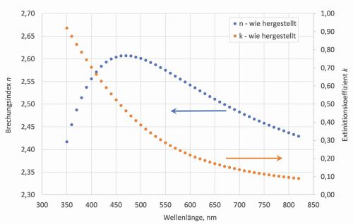 Fig. 4: Refractive index and extinction coefficient of a YIG layer directly after its production Based on the measured spectral curves of Δ and Ψ and using the aforementioned layer model, Figure 4 shows the dependence of the refractive index and the extinction coefficient of the produced YIG thin film on the wavelength; as already noted here for a layer directly after production and without any post-annealing process. These data are in good agreement with the values of other working groups [10, 11].
If we then look at the influence of the yttrium and iron cathode powers on the optical properties of the deposited YIG layers, we find a direct linear relationship between the refractive index n and the set iron cathode powers after evaluating the corresponding ellipsometry measurements on the manufactured layers.
Figure 5 illustrates this very clearly. Measurements were taken here at three different measuring positions over a substrate width of approx. 70 mm in order to be able to assess the homogeneity of the coatings. Against this background, spectral ellipsometry appears to be a suitable method for quantitatively assessing the coating composition after sputter coating.
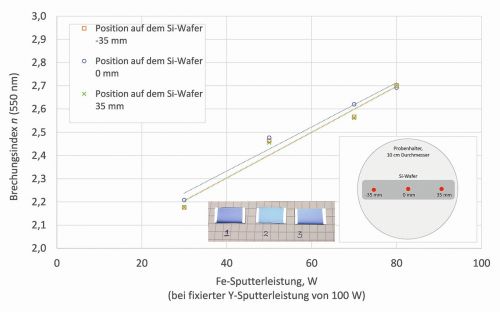 Fig. 5: Refractive index n (550 nm) of YIG coatings as a function of the set iron cathode power at a constant yttrium cathode power of 100 W. The target-substrate distance was 15 cm. Measurements were carried out on three different samples/measurement positions over a substrate width of approx. 70 mm
It should also be noted at this point that the location-dependent local changes in the optical properties (refractive indices, extinction coefficients, layer thicknesses) over the entire possible substrate width of around 70 mm can be documented very precisely. This allowed important conclusions to be drawn with a view to increasing the target-substrate distance from initially 10 to later 15 cm, as a result of which a significantly improved homogeneity was observed for all three parameters mentioned.
Another method used in our investigations to characterize the YIG layers produced is X-ray fluorescence analysis. The method is based on the emission of characteristic secondary (or fluorescent) X-rays from a material sample that is excited with high-energy radiation. On this basis, the method is used for the rapid qualitative and quantitative determination of the elemental composition of this material sample. A mobile XRF spectrometer XL3t 950 He (Analyticon Instruments GmbH) with a silver X-ray tube with an excitation voltage of 50 kV was used for the investigations. In particular, the method was used to determine the exact ratio of the element concentrations of yttrium and iron. In initial investigations, epitaxial YIG layers with known stoichiometry, which were produced by liquid phase epitaxy on GGG substrates [02], were measured. However, since the X-rays penetrate far into the material, emissions are also excited in the substrate material. In order to eliminate the influence of the substrate material, measurements were also carried out on uncoated GGG samples. The adjusted measured intensities result in corresponding correction factors for yttrium and iron. A check of the measurement on other YIG layers with a known composition showed good agreement with the target values.
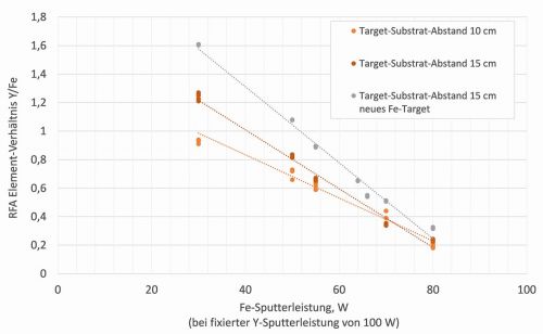
Based on the XRF measurements carried out, the elemental composition of YIG layers deposited on Si wafers could be determined as a function of the cathode power set during layer deposition. Figure 6 shows the Y/Fe ratio of YIG layers on Si wafers determined by XRF over the sputtering power of the iron cathode at constant Y sputtering power. The films were prepared with a target-to-substrate distance of 10 and 15 cm and at room temperature. The oxygen flow rate for all experiments was 5 sccm, which corresponds to an oxygen partial pressure of approx. 3*10-4 mbar.
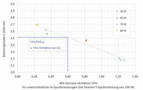
This figure shows an inversely proportional, linear relationship between the impressed Fe sputtering power and the Y/Fe ratio determined by XRF in the resulting thin films. It can also be seen that if the sputtering process conditions are changed, for example by installing a new target or changing the target-substrate distance, the slope of this straight line changes. In this respect, the layer formation process reacts extremely sensitively to such process fluctuations. This makes it all the more important to note that the direct determination of the Y/Fe ratio by X-ray fluorescence analysis on thin YIG layers provides a separate, second possibility to control the stoichiometry in the layers produced and, if necessary, to correct it subsequently by adjusting the parameters (power adjustment) during sputtering. In this respect, Figure 7 summarizes the relationships shown for YIG coatings produced at different iron cathode powers. As already shown, the set iron cathode power has an influence on both the Y/Fe ratio and the refractive index n of the YIG layers produced. Y3Fe2(FeO4)3 or YIG layers with an optimum Y/Fe ratio of 0.6 should have a refractive index n in the range of approx. 2.51 at 550 nm.
To be continued in the July issue.
Literature
[01] G. Schmidt, C. Hauser, P. Trempler, M. Paleschke, E. Th. Papaioannou; "Ultra Thin Films of Yttrium Iron Garnet with Very Low Damping: A Review", Physica Status Solidi B, (2020), 1900644; https://doi.org/10.1002/pssb.201900644
[02] C. Dubs, O. Surzhenko, R. Linke, A. Danilewsky, U. Brückner, J. Dellith, "Sub-micrometer yttrium iron garnet LPE films with low ferromagnetic resonance losses", Journal of Physics D: Applied Physics, 50 (20), 204005, (2017), https://doi.org/10.1088/1361-6463/aa6b1c
[03] S. A. Manuilov, R. Fors, S. I. Khartsev, A. M. Grishin; "Submicron Y3Fe5O12 Film Magnetostatic Wave Band Pass Filters", Journal of Applied Physics, 105, 033917, (2009), https://doi.org/10.1063/1.3075816
[04] C. Dubs, O. Surzhenko, R. Thomas, J. Osten, T. Schneider, K. Lenz, J. Grenzer, R. Hübner, E. Wendler; "Low damping and microstructural perfection of sub-40nm-thin yttrium iron garnet films grown by liquid phase epitaxy", Physical Review Materials, 4, 024416, (2020), https://doi.org/10.1103/PhysRevMaterials.4.024416
[05] B. Bhoi, N. Venkataramani, R. P. R. C. Aiyar, S. Prasad, M. Kostylev; "Effect of Annealing on the Structural and FMR Properties of Epitaxial YIG Thin Films Grown by RF Magnetron Sputtering", IEEE Transactions on Magnetics, 54 (11), (2018); https://doi.org/10.1109/TMAG.2018.2842260
[06] J. Lustikova, Y. Shiomi, Z. Qiu, T. Kikkawa, R. Iguchi, K. Uchida, E. Saitoh; "Spin current generation from sputtered Y3Fe5O12 films", Journal of Applied Physics 116, 153902, (2014), https://doi.org/10.1063/1.4898161
[07] P. Uprety, M.M. Junda, K. Ghimire, D. Adhikari, C. R. Grice, N. J. Podraza; "Spectroscopic ellipsometry determination of optical and electrical properties of aluminum doped zinc oxide", Appl. Surf. Sci, 421, (2017), pp. 852-858, https://doi.org/10.1016/j.apsusc.2017.01.139
[08] L. Fricke, T. Böntgen, J. Lorbeer, C. Bundesmann, R. Schmidt-Grund, M. Grundmann; "An extended Drude model for the in-situ spectroscopic ellipsometry analysis of ZnO thin layers and surface modifications", Thin Solid Films 571 (3), (2014), 437-441, https://doi.org/10.1016/j.tsf.2014.02.010
[09] J. Leng, J. Opsal, H. Chu, M. Senko, D.E. Aspnes; "Analytic representations of the dielectric functions of materials for device and structural modeling", Thin Solid Films 313-314, (1998), 132-136, https://doi.org/10.1016/S0040-6090(97)00799-2
[10] V. Doormann, J.P. Krumme, C.P. Klages; "Measurement of the refractive index and optical absorption spectra of epitaxial bismuth substituted yttrium iron garnet films at UV to near-IR wavelengths", Appl. Phys. A 34, (1984), 223-230, https://doi.org/10.1007/BF00616576
[11] B. Abdel Samad, M.-F. Blanc-Mignon, M. Roumie, A. Siblini, J. P. Chatelon, M. Korek; "Physicochemical characterization of multilayer YIG thin film deposited by rf sputtering", Eur. Phys. J. Appl. Phys. 50, 10502 (2010), https://doi.org/10.1051/epjap/2010026 Figure


