CMOS sensors have established themselves in industrial image processing. A special process enables cost-effective and virtually void-free convection soldering, even for sophisticated CMOS sensors.
The reliable, cost-effective and efficient convection process for soldering CMOS sensors onto PCBs with long-term stability is based on a special process that was developed by E2MS provider Weptech elektronik back in 2011. In recent years, this production technology has been optimized so that current CMOS sensors with significantly increased sensor size can now also be processed. The number of PCBs assembled using this process is now in the 6-digit range - with over 30 different sensor types for well-known camera manufacturers throughout Europe.
New CMOS sensors require a much more careful approach due to increased sensor sizes, higher resolutions and speeds. This leads to a larger number of pins to be contacted with smaller distances and thus to a demanding production process for soldering the sensor to the circuit board.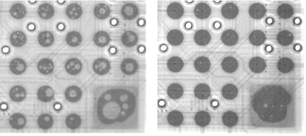 Solder joints with air inclusions with conventional soldering (left) compared to almost pore-free solder joints with the Weptech special process (right)
The sensitive sensors are also challenging to handle and process. In order to ensure that an industrial camera delivers permanently stable images, measures to improve the robustness of the image sensor are already necessary during the production of the hardware. After all, the circuit board must be able to withstand stresses such as temperature cycles or mechanical stress such as vibration.
"Thanks to a special pre-treatment and a new adjustment of the process parameters, the sensors can be soldered in line in a thermally gentle and virtually pore-free manner while strictly adhering to the manufacturer's recommendation. The process is absolutely reproducible and robust. The cameras we have produced in many different batches have proven this in intensive stress tests with a climate chamber, long-term operation and on/off operation," says technology engineer Walter Quinttus.
The E2MS company already exchanges information with its customers during the layout process in order to adapt the circuit board design to the optimized production steps. This saves time and money, especially as the cost of individual CMOS sensors can be quite high.
Since 1994, Weptech has been developing, manufacturing and testing high-quality electronics as part of a comprehensive range of services. Decades of experience in electronics manufacturing and continuous technical development of production methods add up to comprehensive know-how in the areas of SMT and THT assembly, special soldering techniques (e.g. vacuum vapor phase soldering), test development and device assembly. Weptech specializes in the development of new technologies and systems for wireless communication, antenna development and measurement and the certification of radio systems.
