Change in the Board of IMAPS Deutschland e.V.
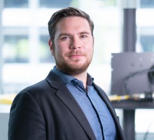
 Since October 2024, Alexander Hensel, M.Sc., has been strengthening the Board of IMAPS Deutschland e.V. in the area of public relations. After studying engineering, he worked for seven years at the Chair of Manufacturing Automation and Production Systems (FAPS) at the University of Erlangen-Nuremberg, where he conducted research in the field of thermal coating processes for power electronics applications. He was also head of the electronics production research department, focusing on data-driven processes and digitalization in SMT and THT production, assembly and connection technology in power electronics and additive manufacturing in electronics production.
As a production technologist, he is currently responsible for flat module production processes at Siemens AG in Erlangen.
FlaMe research project (FKZ: 03EN4008F)
Metal-ceramic substrates (MCS) are important components in power electronic modules and enable long lifetimes with high current carrying capacity. However, due to the widespread manufacturing processes Active Metal Brazing (AMB) and Direct Copper Bonding (DCB), the metallization of MKS is limited to planar metallization and thus offers optimization potential for demand-oriented heat dissipation directly under the heat-generating semiconductor components.
 As part of the FlaMe research project (FKZ: 03EN4008F), copper reinforcements generated additively - by means of laser-based powder bed bonding (PBF-LB/M) - were selectively built up on DCB metallizations and characterized for use in power electronics. The general structure of the power modules under consideration for researching the concept is based on the 2-phase 3RF2 series of Siemens Sirius solid-state relays. In thermal simulations, chips with a spatially limited copper reinforcement of 0.5 mm on the initially 0.3 mm thick DCB topside metallization exhibited a maximum temperature of 81°C at pulsed loads of 3 seconds with a subsequent 3-second pause, which was 26 K lower than the maximum temperature of the same structure without spatially limited reinforcement. The effect was subsequently confirmed in the laboratory, with the maximum temperature of the chip surface measured by thermography at 81 °C being 19 K lower than the comparable setup without amplification. A key aspect that explains the different absolute temperatures between simulation and validation is the occurrence of gas inclusions in the solder layer, as soldering was not carried out in a vacuum atmosphere. In order to analyze the influence of the concept on the service life, comparative load change tests were carried out between unmodified modules and modified modules. It was found that increasing the copper metallization under the chip at a temperature swing of 110 K (40 °C to 150 °C) led to an increase in power loss from 92 W to 109 W on average. On the other hand, the service life was reduced from an average of 26,006 cycles (n=2) to 9,531 cycles (n=3) by reinforcing the chip metallization, which is due to the increased thermomechanical expansion coefficient of the copper as a result of the reinforcement.
 Setup concept for near-chip functionalization of the top-side DCB metallization (left), parameter study for building a dense copper structure without damaging the ceramic (middle) and laboratory setup of the concept for thermal characterization and load cycling tests (right)
Calendar of events
| Location | Period | Event name | Organizer |
| Copenhagen, Denmark | June 10-12, 2025 | NordPac | IMAPS Nordic |
| Grenoble, France | Sept. 16-18, 2025 | IMAPS Europe EMPC 2025 | IMAPS France |
| San Diego, USA | Sept. 29-Oct. 2, 2025 | IMAPS Symposium 2025 | IMAPS USA |
| Munich, Germany | Oct. 16-17, 2025 | Fall Conference | IMAPS DE |
| Phoenix, USA | March 2-5, 2026 | Device Packaging Conference | IMAPS USA |
IMAPS Germany - Your association for packaging and interconnection technology
IMAPS Germany, part of the "International Microelectronics and Packaging Society" (IMAPS), has been the forum in Germany for all those involved in microelectronics and packaging technology since 1973. With almost 250 members, we essentially pursue three important goals:
- we connect science and practice
- we ensure the exchange of information among our members and
- we represent the point of view of our members in international committees.
Imprint
IMAPS Germany e. V.
Kleingrötzing 1, D-84494 Neumarkt-St. Veit
1st Chairman:
Prof. Dr.-Ing. Martin Schneider-Ramelow
Director of the Fraunhofer Institute for Reliability and Microintegration (IZM)
Treasurer
(for questions about membership and contributions):
Ernst G. M. Eggelaar,
Detailed contact information for the board members can be found at www.imaps.de
(Board)


