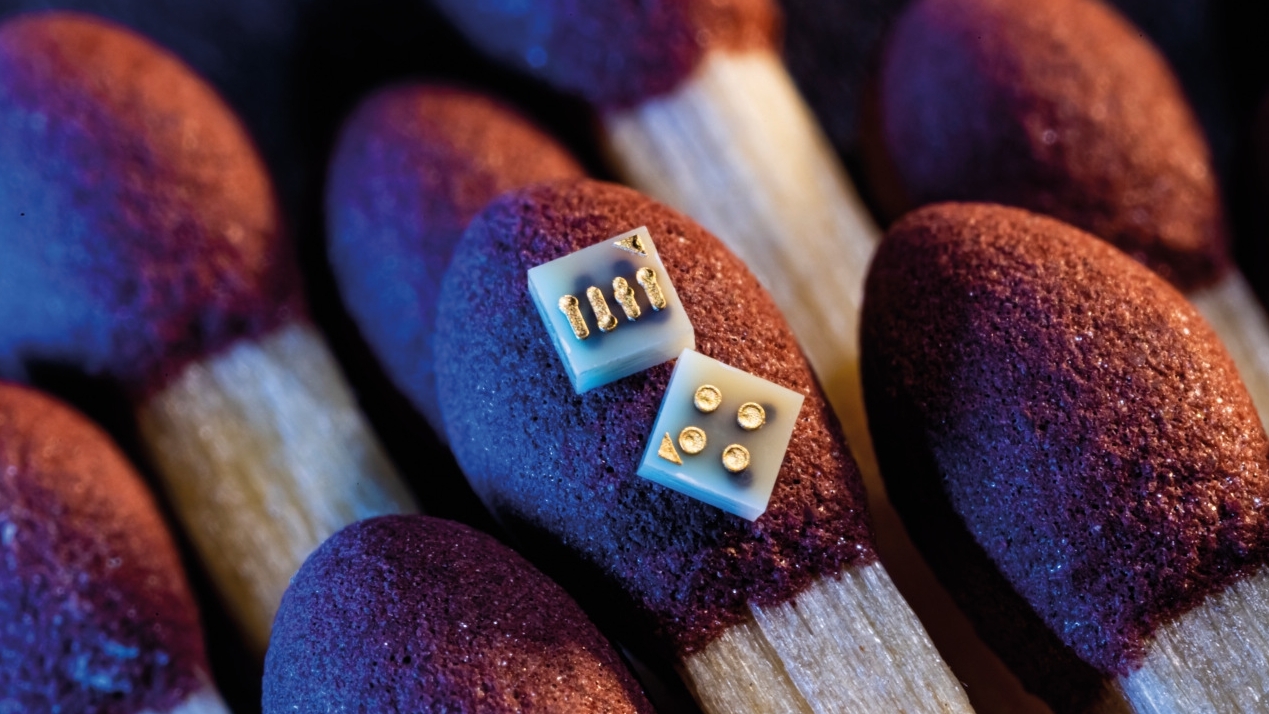
With its digital video output, the digicam image sensor from ams Osram enables visual sensing applications for mobile applications. AT&S has developed the appropriate printed circuit board for this sensor. With a PCB area of 1 mm2 and a weight of around 1 g, the sensor is so compact that it can not only be built into smartphones, VR cameras and other wearables, but can also be integrated into medical applications such as endoscopes.
One of the first products to integrate the AT&S PCB solution is the NanEye camera from ams Osram. It is one of the smallest digital cameras on the market. NanEye can be used for eye tracking in VR glasses and in the medical field. The PCB solution is integrated into a camera head as used for endoscopic examinations.
"With its resolution of 100,000 pixels, the image sensor not only generates sharp images, it also achieves low power consumption thanks to a smart connection architecture," says Markus Maier, Global Account Manager at AT&S. The companies have already worked together on various technology projects in the past.
The hardware design team from AISS (Advanced Interconnect Solution Services) created the layout. The connection design was then realized with ECP (Embedded Component Packaging). ECP enables active and passive components to be integrated into laminate-based high-tech substrates in the smallest possible space. "Instead of placing the components on the PCB, they are integrated into the PCB. They disappear inside the PCB, so to speak," says Maier.
Embedded component packaging (ECP) is made possible by a special manufacturing process. After the respective components have been integrated into a resin layer, they are connected by copper-filled, laser-drilled microvias. This eliminates the need for solder joints for the embedded component. At the same time, finer designs are possible on the outer layer and the components are optimally protected against external influences. With ECP technology, more components can be integrated into the PCB while maintaining the same size of the end device. On the one hand, this increases functionality and, alternatively, the PCB can shrink while retaining the same range of functions.
The NanEye project is an example of products that AT&S intends to offer more frequently in the future. In addition to the technology, the company has also developed the PCB design. "This product fits perfectly into our strategy and shows where our journey is heading," explains Günter Köle, Director Advanced Interconnect Solution Service at AT&S.
