
Three-dimensional electronics concepts have become increasingly important over the last 10 years. However, many questions need to be asked about the corresponding 3D capabilities of design tools. The FED's virtual EDA Round Table dealt with these issues.
Increased performance, miniaturization, functional integration or ergonomic device concepts as well as simpler production can be optimally implemented with 3D electronics. New materials and production technologies such as 3D printing, embedding or plastic electronics, which are now suitable for series production, offer further potential.
But what about design tools and the required data formats? What real 3D design support do electronics CAD tools currently offer? Do they make it possible to exploit the advantages of the new 3D technologies? The Fachverband Elektronik Design (FED e. V.) wanted to find out from the leading EDA manufacturers (EDA, Electronic Design Automation) and therefore invited them to a 'Virtual Round Table'. The manufacturers of the top 5 eCAD systems, i.e. Altium, Cadence, Siemens EDA-Mentor Graphics, Pulsonix, Zuken, briefly presented their new 3D functions and highlights, and the FED working group 3D electronics contributed questions on the design methodology of 3D AVT. Markus Biener, Zollner Elektronik AG, Michael Matthes, Wittenstein SE, and Hanno Platz, GED mbH, moderated the presentation and Q&A session. During the event, which was attended by more than 80 participants, two surveys were conducted on the use and requirements of 3D integration today and in the future. The results were presented at the end.
The printed circuit board becomes the 'conductor body'
3D electronics technologies have become established in series production in several industries in recent years. Driven by the need for more power in a smaller installation space, increasing frequencies, higher reliability and ergonomic device concepts, their use in modern industrial electronics is also becoming increasingly important.
The main advantage of 3D electronics is that, unlike rigid PCBs, the electronic components and connections can also be mounted on curved surfaces of a housing or embedded in the substrate or housing. Replacing individual PCBs with cables and wires with integrated functionality offers many advantages:
- reduced form factor constraints - smaller size
- Reduced weight because PCBs, connectors and cables are no longer required
- Improved electrical performance by reducing parasitic losses
- Easier assembly of electronics, lighting, sensors, SMT components
- Higher reliability by embedding electronics in carriers or housings - Increased resistance to environmental influences such as moisture and vibration
The term 3D electronics stands for multidimensional assembly and connection solutions that can be implemented using different materials and manufacturing processes. In addition to the classic flex and rigid-flex PCBs, which have been used for multidimensional integration for 50 years, a whole range of new assembly and connection solutions have emerged in recent years.
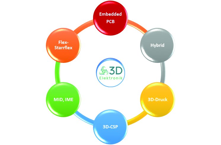 Various new AVT technologies are available for 3D integration in electronics
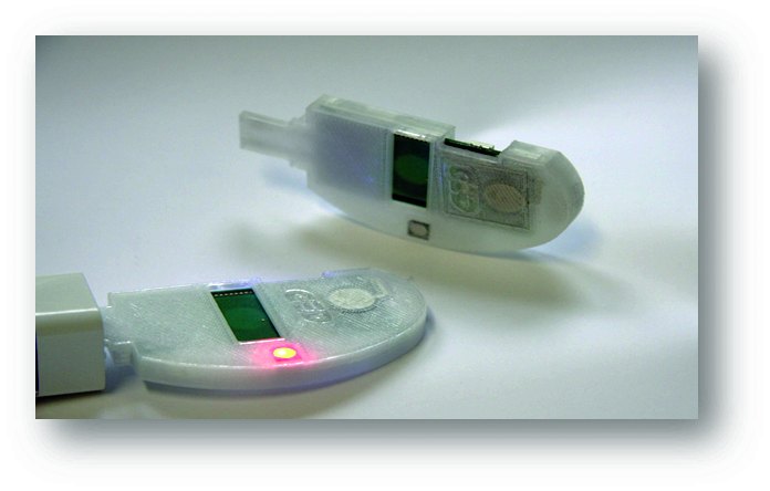 Sensor housing with USB connector, capacitive sensor, LED and antenna produced using 3D multi-material printing
The new AVT solutions for the realization of 3D electronics include
- IME - In Mould Electronics
- MID - injection molding with conductor structures (mechatronic integrated device)
- Embedded PCB - printed circuit boards with integrated components
- 3D hybrid printing, aerosol printing, jet printing
- FHE - Flexible hybrid electronics
- OA - Organic electronics, carriers with integrated sensors or actuators
- Wearable, stretchable electronics
- Functional carriers, e.g. the combination of electronics and fluid technology or optics
Generative manufacturing
Generative manufacturing processes are particularly interesting because they do not require any tools and the electronics can be manufactured practically directly from the CAD system.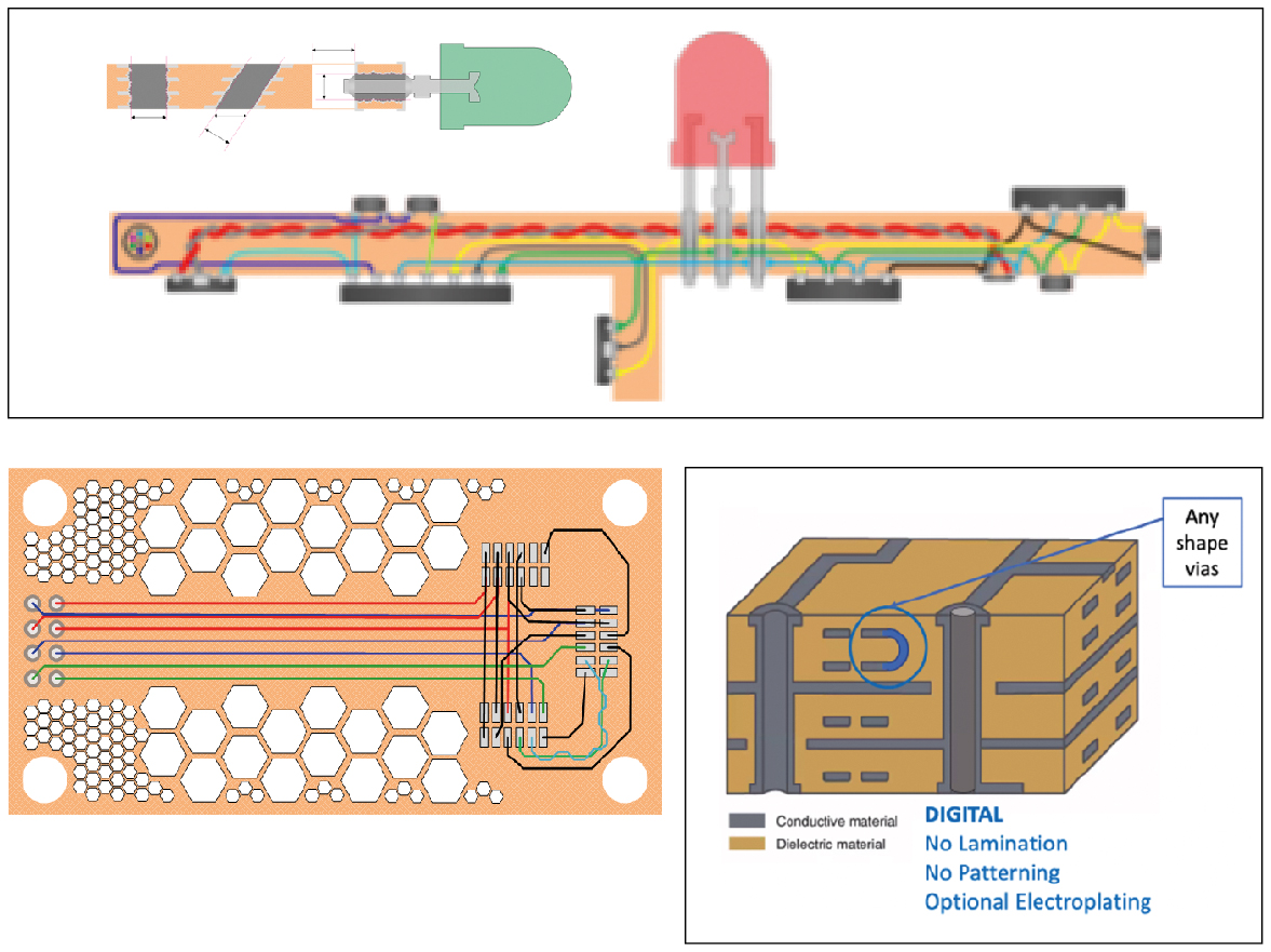 3D: no layers, but connections across the structure as well as bars to increase the creepage distances and any shape vias / Image source: Semikron
The 3D printer makes it very easy to produce changes without new tools or variant production with a series size of 1 piece. Hybrid 3D printers offer the possibility of producing dielectric materials (plastic, ceramic) and conductive materials in one device and one pass. In combination with SMT components or silicon dies, complex multi-layer structures can be realized (embedded components).
Individual eCAD software functionality
Many PCB CAD tools offer support for the PCB design of flex-rigid PCBs. Some already support the embedding of components or so-called 2.5D technologies. For 3D printing or mechatronic integrated devices (MID), however, 'real', i.e. fully comprehensive 3D functionalities of mechanics and electronics are required. This is because components must be able to be placed in all rotations and it must be possible to connect the connections to conductor structures. There are no layers and vias can also be routed across the connection carrier.
What do the CAD tools need to be able to do and how is working in 3D space supported? The challenges are
- No fixed layer reference (Endless Layer, Any Angle Traces)
- No vias, direct connections (vertical fanout for µBGA or bare dies)
- Twisted pair, coaxial shielding, harness design
- Vertical area, conductive 3D area (e.g. EMC shielding LP edge)
- 3D Line/Spacing, 3D DRC, (e.g. min. distance to substrate contour)
- Description of any angle holes, tunnels
- Insulation areas, calculation of paste areas
- 3D spacing rules, insulation bridges, 3D solder mask and much more.
The interdisciplinary tasks of electronics, mechanics, photonics, robotics, bionics, sensor technology and much more will continue to increase rapidly in the future. This will also require a new way of thinking about the design paths of 'organic electronics' for CAD design.
The EDA Round Table made it clear that the following features are absolutely essential for the design of 3D electronics:
- Interoperability of eCAD and mCAD tools, i.e. barrier-free switching between them
- Extended simulation interfaces for field simulation can be called up directly from the EDA systems
- Thermal simulation
- Simulations of the significantly more complex, individual and production-specific design rules
The extent to which artificial intelligence could support or take over the technology design flow was also discussed. However, based on the experience of the last 20 years in the EDA industry, it can be said that only experienced and skilled electronics designers can optimally solve the high complexity of interdisciplinary tasks. However, intelligent, rule- and technology-driven tools can significantly support the work of developers.
The digital twin - design thinking
In the concept phase, it is often not yet clear whether one - and which - of the various 3D AVT solutions is suitable. As in the design thinking process, an iterative evaluation is carried out to determine which solution is optimal for the complex task. The method can be used to develop a superior solution by weighing up economic efficiency, feasibility and desirability. Here too, tools for simulation and verification are urgently needed to support the developer. After all, not every 3D connection solution can be implemented with every technology.
During the discussion, it became clear that all EDA manufacturers involved have developed 3D features in recent years, but are waiting for market demand. Projects such as the embedding PCB project 'HERMES' have often only been implemented in research projects to date. The extent to which the multidimensional tasks compiled by the FED working group on 3D electronics are already supported by EDA manufacturers could not be discussed in the round table due to the limited time frame. Interoperability of systems - Methodological design - Design thinking / Image source: GEDmH
The survey within the round table clearly shows that the trend towards 3D electronics has increased significantly in the last 3 years.
The paradigm shift of digitalization and 'More than Moore' place new, more far-reaching demands on the printed circuit board as well as on the assembly and connection technology. The combination of digital and analog technology, the connection of silicon chips to analog and high-frequency components, high-voltage and high-voltage components, sensors and actuators will pose major challenges for developers and EDA tools in the coming years. Integration in the third dimension is required more and more frequently.
Heterogeneous integration with 3D electronics
In the BMBF research project 'FreiForm', GED mbH, together with the Fraunhofer Institute IZM, Schaeffler and other partners, developed concepts with various AVT solutions for an IoT sensor with free shaping. The partners successfully developed three different technology demonstrators with varying degrees of integration. Thanks to the '3-dimensional' free-form solution, an IoT multi-sensor including BLE antenna and energy harvesting in a size of 8 x 20 mm was realized using 3D CSP technology.
Which 3D-eCAD data formats?
Data in IDF, STL or GDSII formats is required for production for the various manufacturing processes such as 3D printing, 3D CSP and hybrid flex. The generation of the different 3D production formats was therefore also an important topic. The different technologies are manufactured using completely different machines and materials. Gerber data is not useful here. The MID process, for example, requires a data set for the housing in STEP format and one for the conductor structures in IDF format. Opinions differed on the extent to which the IPC 2581 format propagated by the IPC meets all 3D requirements. In international standardization bodies such as DKE and IEC, the working group is actively involved in defining the design rules and data formats, represented by FED member Michael Schleicher. The FED is also active in the IPC 2581 committee in the USA.
Result of the EDA Round Table
Rule-based, high-performance CAD and simulation tools with an extended range of functions are urgently needed for the rapid, successful development of complex 3D electronics - manufacturers are called upon to act. The participants expect EDA manufacturers to provide more technology support from the CAD tool, starting with simple standard rules such as IPC classes 1/2/3 or standardized distances for voltages and conductor widths for power electronics. But technology rules for in-mold technology (IME), embedded PCB and others are also on the wish list. The participants would like to see the EDA Round Table in this form once or twice a year, and the manufacturers should also demonstrate their 3D functions using very specific examples, which they would then preferably present live.
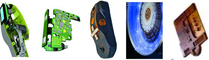 PCB + complex housing, Flex PCB + Housing (fold & stack), Mechatronic Interconnect Device, In Mold Electronics, 3D Printed Electronics / Sources: All3DP, Zollner, 3D-MID e. V.,Tacto Tek, Nano Dimension, Signify Research
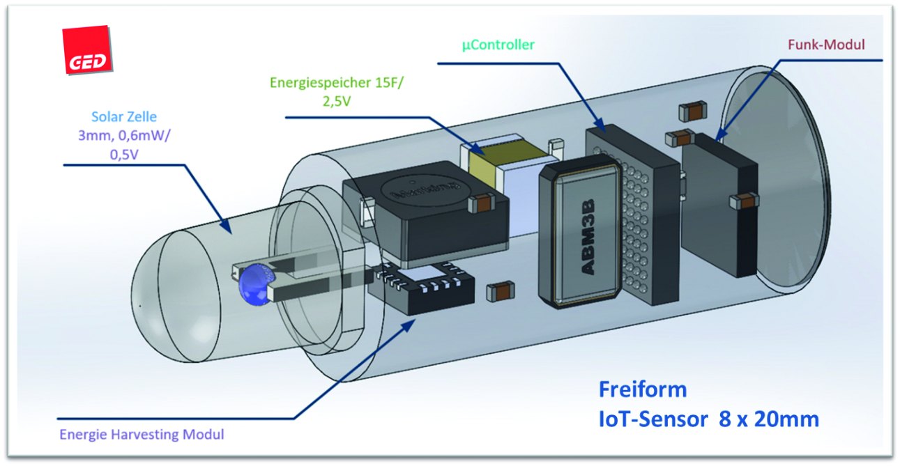 IoT multisensor " including BLE antenna and energy harvesting / Image source: GEDmbH
According to IDtechEx, the market for 3D electronics is expected to double in the next 5 years and even triple by 2030. The demand is there and the European electronics industry needs to address the issue now.
