High voltage poses a risk to life and limb, but also to printed circuit boards. The force of higher voltages is needed for electrical drives, but this force can also be destructive.
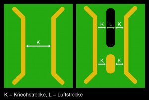
 Fig. 1: Creepage distances extended by an air gap or shortened by an island Image: FlowCADIn order tomake line electronics safe, the distances between conductive materials must be large enough between high voltage potentials to prevent arcing or breakdown.
The safety regulations on clearance and creepage distances and dielectric strength are primarily intended to protect human life. Wherever people are transported and their lives may be at risk, there are special standards for maintaining safety distances at high voltages. These applications include elevators, vehicles and airplanes, but also medical technology. Compliance with clearance and creepage distances as well as dielectric strength is important, as it is not only the electronics themselves that can be destroyed. Their failure or malfunction can have catastrophic consequences for people. When it comes to people (lives), the issues of liability and insurance cover are of major importance to manufacturers.
The number of developments in electric drives is increasing rapidly due to the trends towards e-mobility, automation and renewable energies, and new suppliers are also entering the market. Control units for electric motors are no longer only used stationary, but also mobile in vehicles. Power semiconductors such as IGBTs, MOSFETs or SiC diodes with higher voltages are used to optimize the efficiency of control units. Depending on the application, there are different maximum values for low, medium and high voltage. In order to protect people or systems from the effects of electrical malfunctions, particularly in the event of an overvoltage, sufficient dimensioning of the clearances and creepage distances as well as the dielectric strength is required.
What is a clearance or creepage distance?
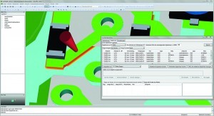
 Fig. 2: Evaluation of areas with insufficient dielectric strength Image: FlowCAD Aclearance distance is the shortest distance between two electrical conductors through the air. If a high voltage is applied to both conductors, the air in between is ionized and becomes more conductive. Depending on the surge voltage, contamination, duration and air pressure, a short circuit can occur through the air and an arc can be seen. Arcing results in high temperatures, an electromagnetic field and an unplanned transfer of charge between the two conductors. These influences can destroy the electronics or neighboring components. The dimensioning of the clearances is based on the rated surge voltages, which are derived from the overvoltage category and the applied voltage.
In the case of a creepage distance, a short circuit occurs between two conductors on the surface of the insulation material if the effective voltage is exceeded. In the case of printed circuit boards, the current 'creeps' on the surface of the FR-4, protective lacquer, components and cables. A creepage distance is the shortest connection along the surface of the insulator between the conductors.
Humidity and air pressure affect the flashover voltage through the air and the likelihood of arcing. Moisture, oils and dust are deposited on the surfaces of the PCB and components and reduce the insulation distances between the conductors over time.
If the distance between two conductors on the PCB is too small and the permitted creepage distance is not reached, a slot can be milled between the conductors(Fig. 1 top right). The permitted distance is then calculated from the combination of clearance and creepage distances. With the NEXTRA software, the distance is not only checked on one level. As the creepage current can also creep upwards or downwards in a routing, hole or PCB edge, possible voltages to conductors on other layers along the surface must also be checked in three dimensions.
Copper islands, fixing screws or other conductors located between the two conductors with higher voltages shorten the distance(Fig. 1 bottom right). In the standards, conductive elements between the conductors under consideration are referred to as three-point problems or discontinuities. For a test, all combinations and paths at the edge of holes must be checked.
The value for the dielectric strength or the necessary distance for the required clearance and creepage distance depends on
- Degree of soiling
- air humidity
- temperature
- Air pressure
- Overvoltage category
- Frequency
- Chemical loads
- Hydrolysis
- Mechanical pressure
- Area of application (automotive, aerospace, household, industry or medicine)
Various standards discuss the safety of live parts in low-voltage systems and define corresponding safety distances. Examples are listed in DIN EN 60664-1/VDE 0110. This standard defines the distances to be maintained between conductive objects in order to prevent a creepage distance, flashover or breakdown.
The IEC 61010 standard defines any contamination with gases, liquids or solids that can lead to a reduction in the electrical resistance or insulation capacity of an isolating distance as contamination. The specified distances are divided into the following categories depending on the degree of contamination:
- Pollution degree 1: allows no or only slight, but non-conductive pollution. The contamination has no influence.
- Degree of soiling 2: is light, normal soiling that can become conductive through occasional condensation or hand perspiration.
- Contamination degree 3: is a contamination that is conductive or becomes conductive through condensation.
- Pollution degree 4: permanent conductivity caused by conductive dust, rain or moisture (but no longer acceptable for insulation that is a protective measure).
Dielectric strength
The dielectric strength of an insulating material describes the maximum electric field strength (in kV/mm) before a voltage breakdown occurs. The FR-4 material insulates the superimposed layers of printed circuit boards and has a dielectric strength of around 13 kV/mm at an ambient temperature of 20 °C. Moreover, the breakdown voltage of many materials is not proportional to the thickness of the insulator, as inhomogeneous field distribution can occur, especially with DC voltage. For this reason, thin films have higher dielectric strengths than thicker materials. This effect is utilized in film capacitors, for example. The dielectric strength depends on various factors. The value decreases with increasing temperature and increasing frequency and is therefore not a material constant. A 3D simulation with finite elements is required for testing.
High voltage starts at a voltage above 60 V
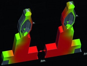
 Fig. 3: NEXTRA alerts the user to connectors that are placed too close together Image: FlowCADIn theCAD flow, the distances must already be provided for in the layout and layer structure. Layout software usually only checks the spacing on one layer and ignores islands or routing. NEXTRA is software that can read in design data from different eCAD systems and then perform a standard-compliant check of the PCB. Component models and enclosure design data can also be imported into NEXTRA via direct bidirectional interfaces for all major eCAD and mCAD systems to fully verify the air gaps.
3D STEP models for components can be imported directly from Allegro or OrCAD, for example, and conductive or insulating material information is automatically transferred via color codes without having to create an intermediate database. The accuracy can be set for exact geometric analysis with finite elements.
In the automotive industry, the new generation of electric and hybrid vehicles uses battery voltages of 400 V and even 850 V, and higher voltages are also used in inverters. In the automotive sector, voltages above 60 V are referred to as high voltage. The differentiation of voltage classes into extra-low, low, medium, high and extra-high voltages comes from installation and building technology. Until now, a distinction has only been made between low and high voltage in automotive engineering in order to give mechanics in the workshop a special indication of the electrical hazards. High-voltage components must have a dielectric strength in accordance with ISO 6469 due to the design of the system.
Problematic voltage peaks
Frequency converters and switched-mode power supply units now place greater stress on insulation than in the past, as motor control units or power supply units use pulse-width-controlled square-wave voltages in the range of 20 kHz and more. The resulting harmonics have frequency components of well over 50 MHz. In addition, resonances and inductive or capacitive coupling, for example, result in peak voltages far above the operating voltage. The high switching speeds (du/dt) in the power electronics of MOSFETs or IGBTs place considerable strain on the insulation materials used.
In addition to internal circuit factors such as high frequencies, there are also external factors when switching with power semiconductors. Inductive loads that are switched or the capacitance of connected cables cause unwanted voltage peaks. The maximum values of the voltage peaks caused by external factors can be determined in advance by circuit simulations with PSpice and recorded as peak voltage in the CAD data and used for voltage tests.
Mechanical tolerances must be taken into account for a statement on safety. Not only the shortest path is identified, but also a range that could be problematic with the given input parameters such as stress, material, contamination and air pressure. The influence of manufacturing and assembly tolerances is taken into account in NEXTRA. Figure 3 shows that the two surfaces of a connector can be placed too close together due to manufacturing tolerances. Such tolerances can only be detected by chance when testing prototypes.
Increasing reliability
 Fig. 4: Dendrite formation on an insulator along the creepage distance Image: Department of Engineering - University of LeicesterCircuitsimulation and verification of clearances and creepage distances can improve reliability and conformity with standards. It is difficult to test breakdown and flashover in the installed state with different levels of contamination. In a professional CAD flow, the 3D STEP models for high-voltage components should have different color codes for conductive and insulating materials. This makes it quick and easy to start an air and creepage distance analysis together with the netlist, peak voltages and specifications for contamination classes. The PCB designer can then develop reliable circuits and avoid thermal destruction due to air gaps and creepage distances.
The insulation coordination consists of an investigation of the air and creepage distances and the dielectric strength. A simulation can take into account all the shortest paths with all the parameters. However, the accuracy of the simulation can only be as good as the input parameters. One input parameter is contamination, which is only verbally divided into four categories. NEXTRA therefore treats insulation violations as 'problematic areas', which are reserved for final engineering assessment. A simple shortest path does not usually occur in reality, as the insulation material, electric fields and contamination are not homogeneous. Images of creepage distances show fractal structures (dendrite formation, Fig. 4). Therefore, the entire problematic area must be subjected to a final engineering assessment.
Insulation clearances from voltages of 60 V should already be checked in the PCB layout, as this allows all combinations and manufacturing tolerances to be simulated at an early stage. And any weak points identified at an early stage can be rectified without incurring follow-up costs.


